


")
-
- Products, devices, systems, plants for applications
RFID Operator Identification for Secure Processes in Semiconductor Manufacturing
The HERMOS HFS E-Sign Reader
In semiconductor manufacturing, seamless traceability, unique operator identification, and standardized processes are essential prerequisites for consistently high product quality. Especially at manual workstations, reliable operator identification ensures that process steps are clearly documented a…


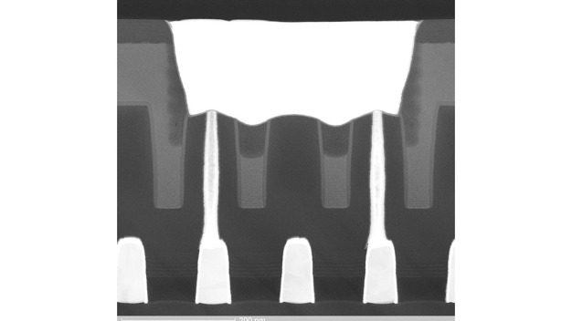
 conventional via-middle and (right) local-BDI TSV approaches, assuming a cell height of 115nm and bulk Si thickness of 500nm.")

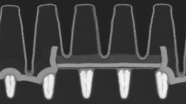
 X-cut HAADF STEM for a WS2 device with a CPP of 50nm, a contact length of 19nm and width of 256nm, after gate connection line etch. And (B) corresponding energy dispersive X-ray spectroscopy (EDS) EDS analysis.")
, integrated on the same 300mm wafer, show proper threshold voltage matching.")


")
")
")
")
")
")
")
 and barrier (B) gates of barely 6 nanometers, enabled by High NA EUV lithography. The image also shows the accumulation gates (A) and confinement (C).")


