




- Know How, Institute
- Translated with AI
Wolfgang Richter
TU Berlin paves the way for mass production of quantum chips
By precisely placed quantum dots, quantum light sources can be integrated onto semiconductor chips in a scalable and reproducible manner for the first time
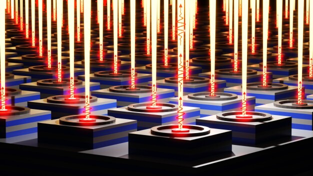
Schematic representation of a scalable platform composed of quantum light sources, where precisely positioned quantum dots are integrated into nanoresonators.
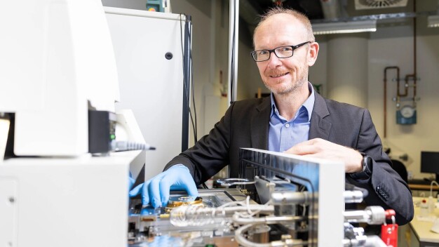
Prof. Dr. Reitzenstein in front of the sample chamber of the electron beam lithography system, which produces highly precise nanostructures for scalable next-generation quantum light sources.
Optical quantum chips are considered key components of future communication and computer technologies. Their production has so far been complex because the sources needed for individual particles of light – so-called semiconductor quantum dots – formed randomly on the chip and initially had to be located painstakingly. Researchers at the Technical University of Berlin have now developed a solution to this problem: by controlled integration of "stressors" into the substrate, they can generate material stresses on the surface precisely enough to grow artificial atoms in the form of semiconductor quantum dots at targeted locations. This creates the foundation for scalable and industry-compatible manufacturing of optical quantum chips.
The work was conducted under the leadership of Prof. Stephan Reitzenstein in the "Optoelectronics and Quantum Devices" working group at the Institute of Physics and Astronomy at TU Berlin, in collaboration with researchers from the Carl von Ossietzky University Oldenburg. The scientists developed a new quantum chip architecture in which the so-called quantum dots – nanoscale semiconductor structures for generating individual particles of light – are precisely integrated at predefined positions within the chip. The results were published in the journal Light: Science & Applications.
From Randomness to Targeted Production
Quantum dots are considered promising sources of individual particles of light (photons). Such particles are an important basis for future applications like secure quantum communication, quantum networks, quantum sensing, or photonic quantum computers. However, a central problem has so far arisen during production: the quantum dots formed randomly during the growth process on the semiconductor material. Researchers first had to identify suitable quantum dots painstakingly before they could fabricate the necessary photonic structures around them. "This approach was very successful for individual demonstrators. However, if you want to produce many quantum light sources of comparable quality on a chip, the random positioning of the quantum dots becomes a major bottleneck," explains Kartik Gaur, who developed the quantum device components as part of his doctoral thesis. "Our approach shifts this step already into the crystal growth: the quantum dots form where they are later needed in the photonic device."
The research group led by Prof. Reitzenstein thus developed a method that predetermines the position of the quantum dots during crystal growth. This is made possible by a special, hidden layer within the chip's substrate, which generates very precise material stresses and thus directs the growth of the quantum dots. Subsequently, the quantum dots are integrated directly into nanophotonic resonators that collect the generated light very efficiently and make it available for quantum technology applications.
High Yield and Reproducible Quality
Using the new method, the researchers fabricated a 6x6 grid of 36 quantum light sources, all of which were functional. This achieved excellent reproducibility, which has been rarely attained in semiconductor-based quantum photonics so far. "The real significance of this work does not lie solely in the high yield of the devices," says Reitzenstein. "It is crucial that we can demonstrate how powerful quantum light sources with controllable quality and high reproducibility can be realized on a semiconductor chip. This addresses a central challenge in quantum photonics: the transition from individually optimized laboratory demonstrators to scalable, technologically usable platforms for future quantum systems."
Foundations for the Next Generation of Quantum Chips
Furthermore, the research team investigated in detail how small deviations in the positioning of the quantum dots affect the performance of the devices. To do this, the researchers combined various imaging, spectroscopic, and quantum optical measurement techniques with numerical simulations. The theoretical work was carried out by the group led by Prof. Christopher Gies at the Carl von Ossietzky University Oldenburg. The modeling explains how the precise position of the quantum dots influences the properties of the generated particles of light and provides important guidelines for developing future quantum chips.
Demonstrated High Quality of the Quantum Light Sources
The team also quantitatively demonstrated the performance of the quantum light sources. For the best devices, nearly half of the generated particles of light could be coupled out of the chip for further use – a very good value. At the same time, the quantum "purity" of the individual particles exceeded 99 percent. Additionally, the generated particles of light exhibited nearly identical quantum optical properties. This is an important prerequisite for future photonic quantum computers and quantum networks, where many particles of light must interact in exactly the same way.
Additional Information:
Scalable quantum photonic platform based on site-controlled quantum dots coupled to circular Bragg grating resonators, Kartik Gaur, Avijit Barua, Sarthak Tripathi, Léo J. Roche, Steffen Wilksen, Alexander Steinhoff, Sam Baraz, Neha Nitin, Chirag C. Palekar, Aris Koulas-Simos, Imad Limame, Priyabrata Mudi, Sven Rodt, Christopher Gies & Stephan Reitzenstein
https://www.nature.com/articles/s41377-026-02343-0
Technische Universität Berlin
10587 Berlin
Germany