


- Electronics (wafers, semiconductors, microchips,...)
- Translated with AI
ASML, TSMC and imec bring industry-ready 2D-material transistors closer with breakthrough 300mm integration
Novel 300mm integration approach for 2D-material based devices enables scaled n and pFETs with 50nm contacted poly pitch.
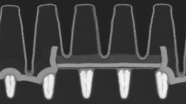
 X-cut HAADF STEM for a WS2 device with a CPP of 50nm, a contact length of 19nm and width of 256nm, after gate connection line etch. And (B) corresponding energy dispersive X-ray spectroscopy (EDS) EDS analysis.")
Figure 1 - (A) X-cut HAADF STEM for a WS2 device with a CPP of 50nm, a contact length of 19nm and width of 256nm, after gate connection line etch. And (B) corresponding energy dispersive X-ray spectroscopy (EDS) EDS analysis.
, integrated on the same 300mm wafer, show proper threshold voltage matching.")
Figure 2 – MoS2 nFETs and WSe2 pFETs with 50nm contact pitch and relaxed channel width (650nm), integrated on the same 300mm wafer, show proper threshold voltage matching.
– ASML, TSMC, and imec introduce an innovative 300-mm integration process for transistors based on 2D materials, enabling the first scalable n- and p-FETs with a contact pitch (CPP) of 50 nm, structured using EUV lithography.
– Good results were achieved with scaled nFETs (with MoS2 channel) and pFETs (with WS2 or WSe2 channels): both transistor polarities turn off at a gate voltage (Vg) of 0 V, and the pFETs demonstrate performance close to that of the most advanced laboratory devices.
– This development is a crucial step in transitioning from laboratory to mass production of transistors based on 2D materials, which are expected to further expand and improve the roadmap for logic technology.
– “Together with our partners, we have established a 300-mm test platform to investigate 2D materials at dimensions relevant to industry. We invite the semiconductor ecosystem to collaborate in further advancing the performance of this new class of channel materials and devices.” – Gouri Sankar Kar, imec.
This week, imec, a globally leading research and innovation center for advanced semiconductor technologies, presents at the IEEE/JSAP Symposium 2026 on VLSI Technology and Circuits, in collaboration with lithography solutions provider ASML and semiconductor foundry TSMC, a novel, robust, and scalable 300-mm integration approach for n- and p-FETs based on 2D materials. For the first time, scaled nFETs (with MoS2 as the channel material) and pFETs (either based on WS2 or WSe2) with a contacted poly pitch (CPP) of 50 nm have been demonstrated, showing good current-voltage characteristics. These results represent a significant step in moving from laboratory to industrial-scale manufacturing of 2D-material-based transistors, intended for ultra-scaled logic as well as back-end and wafer backside applications.
Two-dimensional transition metal dichalcogenides (TMDs, such as MoS2, WS2, and WSe2) have the potential to extend and improve the logic scaling roadmap. When integrated as atomically thin conduction channels replacing silicon, these materials enable high-performance scaled transistors—attractive for both extremely scaled logic and back-end-of-line and wafer backside applications. This potential is due to their good electrostatic control of the channel combined with acceptable charge carrier mobility, even at extremely reduced gate and channel lengths. However, the path to industrial adoption has been hindered so far by the lack of a 300-mm integration process capable of delivering TMD-based n- and p-FETs in industry-compatible dimensions without compromising the performance already demonstrated at the laboratory scale.
ASML, TSMC, and imec now present a scalable, back-end compatible 300-mm integration approach for TMD-based n- and p-FETs, which has led to three key results: (1) scaled n- and p-FETs with a contact pitch (CPP) of 50 nm—worldwide unique; (2) very low off-current (Ioff) at a gate voltage of zero (Vg=0V) for both transistor polarities; and (3) pFETs with WSe2 channels, whose performance approaches that of record-breaking laboratory devices. With 94% functional transistors (i.e., with Imax/Imin > 10^5), the CMOS-like integration approach—where n- and p-FETs are integrated on the same 300-mm wafer—has proven to be robust and stable. The proposed process flow is applicable to other 2D channel materials beyond MoS2, WS2, and WSe2.
Gouri Sankar Kar, Vice President of Research and Development in Computing and Storage Technologies at imec: “Transistors based on 2D TMD materials are typically optimized for short channel lengths. However, they usually have a large contact area to keep contact resistance as low as possible, which makes further miniaturization difficult. For the first time, we have achieved a CPP of 50 nm—a metric determined by both the gate length and the source/drain contact length—without compromising the performance of the 2D n- and p-FETs. The use of single-pattern EUV lithography, optimized in close collaboration with ASML, was crucial in enabling the scaled CPP.”
The scaled transistors exhibit good current-voltage characteristics, with pFETs performing almost as well as the most advanced laboratory devices—addressing a long-standing challenge for TMD transistors. Furthermore, electrical measurements show that both transistor polarities turn off when the gate voltage (Vg) is set to 0 V. “This ideal behavior can be attributed to the use of an innovative ‘reversed’ manufacturing process for thin-film transistors (TFTs),” explains Gouri Sankar Kar. “Unlike conventional transistors based on 2D materials, our n- and p-FETs feature bottom contacts and an overlapping gate. This is achieved by depositing the TMD channel material onto pre-structured trenches filled with tungsten (W), which serve as contacts.”
Dr. Min Cao, Vice President and CTO of TSMC, emphasized the strategic importance of the research and stated: “Our research collaboration plays a crucial role in pushing the boundaries of semiconductor innovation. The focus is on risk reduction and accelerating the transition from laboratory to manufacturing to ensure that groundbreaking discoveries—particularly in this new class of channel materials—are quickly and efficiently integrated into advanced manufacturing, ultimately leading to innovative solutions.”
“2D TMD materials could potentially enable significantly smaller and more powerful transistors than silicon-based ones, but the devices demonstrated so far using 300-mm processes are quite large and structured with older lithography technologies. Thanks to the much higher resolution of EUV lithography, we were able to produce TMD transistors with channel lengths of only 28 nm and pitches compatible with the most advanced transistor nodes,” added Etienne De Poortere, Director of the Technology Development Center Europe at ASML.
IMEC Belgium
3001 Leuven
Belgium


