



- Translated with AI
ZEISS invests an additional 60 million euros in the expansion of the semiconductor technology plant
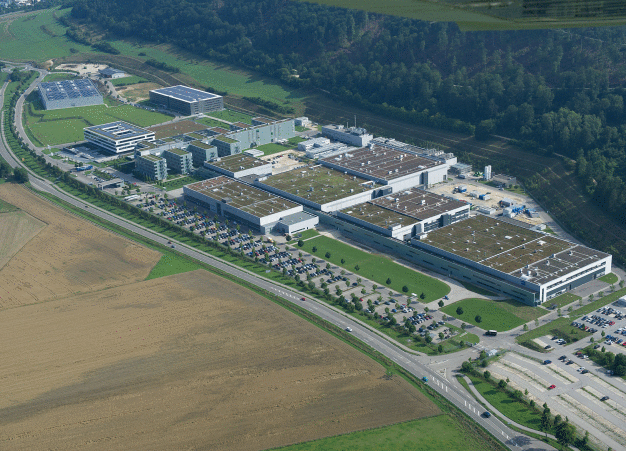
The world's most modern center for lithography optics is set to expand: ZEISS's Semiconductor Manufacturing Technology (SMT) division plans to extend its manufacturing capabilities in the inter-municipal industrial park Oberkochen/Königsbronn.
- The world's most modern center for lithography optics in Oberkochen to be expanded by 6,000 square meters
- Building application for expansion submitted
The world's most modern center for lithography optics is set to grow further: ZEISS's Semiconductor Manufacturing Technology (SMT) division plans to expand its manufacturing capabilities in the inter-municipal industrial area Oberkochen/Königsbronn. A corresponding building application has been submitted to the responsible municipal council. The plan includes expanding existing production areas as well as constructing a new hall for the next generation of lithography optics using extreme ultraviolet light (EUV). This requires even higher manufacturing standards and is expected to be available at the beginning of the next decade for the production of new high-performance chips.
Dr. Hermann Gerlinger, member of the Executive Board of Carl Zeiss AG and head of the Semiconductor Manufacturing Technology division, explains: "ZEISS continues to work intensively on realizing innovative EUV lithography for the manufacturing of tomorrow's microchips. The positive market signals of recent months reinforce our commitment to invest further in this future technology beyond the current generation. This demands even higher levels of our technological expertise—and our infrastructure."
Overall, ZEISS's Semiconductor Manufacturing Technology division plans to invest more than 60 million euros in the upcoming expansion of the lithography optics center over the next few years. The production areas will be expanded by approximately 6,000 square meters.
Used in wafer scanners for the Dutch customer ASML, EUV lithography optics enable the production of even more powerful microchips.
The completion of the new production areas is scheduled for 2018.
ZEISS Gruppe
Germany