New year, new job? View the vacancies! More ...
Systec & Solutions GmbH MT-Messtechnik ClearClean Pfennig Reinigungstechnik GmbH


All publications for the rubric Electronics (wafers, semiconductors, microchips,...)

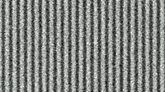
The TWINSCAN EXE:5000 High NA EUV scanner in the High NA Lab demonstrating the first-ever 10 nm dense lines obtained in a single exposure.
  • Electronics (wafers, semiconductors, microchips,...)

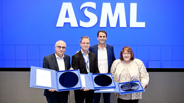
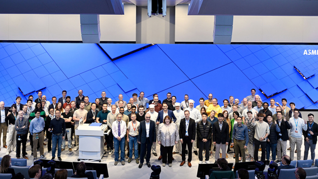
Opening of the joint ASML-imec High NA EUV Lithography Lab marks a milestone in preparing High NA EUV lithography for accelerated adoption in mass manufacturing

ASML and imec open joint High NA EUV Lithography Lab offering an early development platform to the leading-edge semiconductor ecosystem

Imec, a world-leading research and innovation hub in nanoelectronics and digital technologies, and ASML Holding N.V. (ASML), a leading lithography supplier to the semiconductor industry, today announced the opening of the High NA EUV Lithography Lab in Veldhoven, the Netherlands, a lab jointly run b…

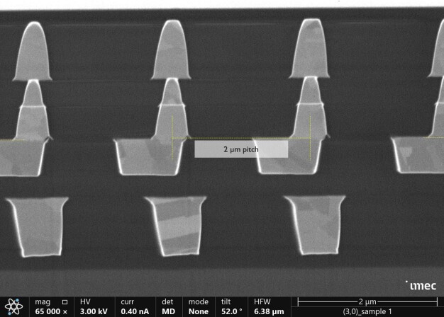
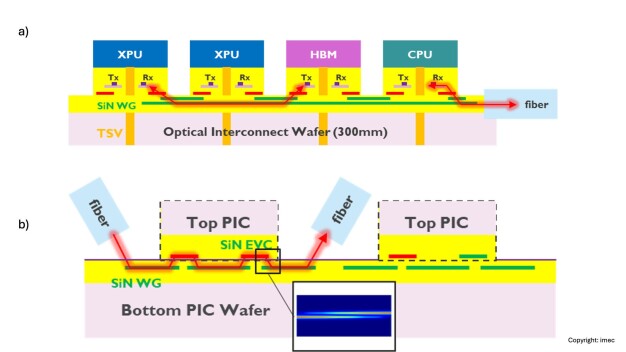
Figure 1 – Cross-section SEM image of a die-to-wafer hybrid bonded test vehicle with 2µm bond pad pitch. Figure 2 – A) Vision for an optically interconnected multi-XPU computing system at wafer level; and B) demonstrated test system consisting of PIC dies with embedded SiN waveguides (WG) and evanescent couplers, connected to a bottom PIC wafer with complementary SiN evanescent couplers.
  • Electronics (wafers, semiconductors, microchips,...)

Improved die-to-wafer assembly flow opens doors to logic/memory-on-logic stacking, and to optically interconnected systems-on-wafer

Imec demonstrates die-to-wafer hybrid bonding with a Cu interconnect pad pitch of 2µm

This week, at the 2024 IEEE Electronic Components and Technology Conference (ECTC), imec, a world-leading research and innovation hub in nanoelectronics and digital technologies, presents a Cu-to-Cu and SiCN-to-SiCN die-to-wafer bonding process resulting in a Cu bond pad pitch of only 2µm at <350…

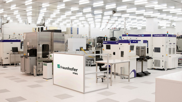
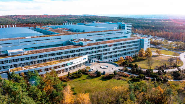
300 mm cleanroom at the Fraunhofer IPMS. © Fraunhofer IPMS Aerial view of Infineon Dresden. © Infineon Technologies AG / Aerial view of Infineon Dresden. © Infineon Technologies AG
  • mobility of the future

Intelligent energy management for the future

Fraunhofer IPMS supports the 300 mm process development of smart power technologies for the semiconductor manufacturer Infineon at the Dresden site

In a joint development project spanning around one year, important progress was made in the production of “Smart power technologies”. Fraunhofer IPMS provided significant support to the semiconductor manufacturer Infineon by supplying selected process modules within the entire CMOS process value cha…

5DOF Miniature XYZ-Phi-Delta Positioning System for active alignment and mounting of optics. (Copyright: Steinmeyer Mechatronik)
  • Electronics (wafers, semiconductors, microchips,...)

High-precision positioning system for active alignment and mounting of optics

Innovative 5-Axis Aligner for the Semiconductor Industry

With the 5DOF Miniature XYZ-Phi-Delta Positioning System, Steinmeyer Mechatronik offers an innovative solution for highly precise alignment processes. The combination of a tripod and XY cross table guarantees maximum precision, robustness, and reliability, while also impressing with its compact desi…

Better informed: With YEARBOOK, NEWSLETTER, NEWSFLASH, NEWSEXTRA and EXPERT DIRECTORY

Stay up to date and subscribe to our monthly eMail-NEWSLETTER and our NEWSFLASH and NEWSEXTRA. Get additional information about what is happening in the world of cleanrooms with our printed YEARBOOK. And find out who the cleanroom EXPERTS are with our directory.

Berner International GmbH Vaisala C-Tec Piepenbrock