


- Company
- Translated with AI
AP&S establishes location in the USA
")
In a facility, wafers are processed to produce microchips. Here is a so-called batch system that can process multiple wafers simultaneously. (Image: AP&S)

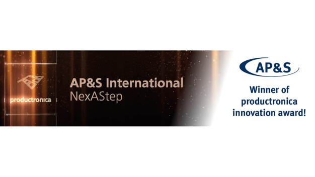
The wet process system "NexAStep" won the "productronica innovation award" in 2023. (Image: AP&S)

The company based in Donaueschingen (Aasen) announces its market entry into the USA. In response to customer inquiries from the USA, AP&S has now implemented this step and has already hired its first employees as of April.
AP&S International GmbH manufactures wet process equipment for the production of microchips and is thus active in the semiconductor industry. The USA remains a key market for German machinery manufacturing, and semiconductors have also moved to the center of geopolitical interests. Additionally, the "Chips Act" is attracting chip corporations and suppliers to the USA.
With a gross domestic product of around 27.97 trillion US dollars (2024), the USA is the world's largest economy. The opportunities for companies are accordingly great in the land of unlimited possibilities.
One of the drivers for investments in the USA is the expected boom in electric vehicles. Producing SiC chips can guarantee higher range and more efficient charging processes. This technology is also being strongly promoted in the USA.
The currently 250-employee company AP&S has over 20 years of market expertise, giving it the know-how for market expansion. Potential customers based in the USA are usually already familiar with the company through existing contracts with other locations worldwide. As a result, the first major order has already been placed for five systems, which will be built for a customer in the USA by mid-2025.
The systems ordered for the USA include both production-supporting equipment and batch systems (where multiple wafers* are processed simultaneously), some standardized and some customized to customer specifications. To realistically test and prepare customer processes, the company has a demo center where laboratory tests are conducted to precisely prepare the wet processes for the systems. Operator training is provided at the in-house training center, the AP&S Academy, helping to address the skilled labor shortage.
Tobias Bausch, CMO & CTO of AP&S International GmbH, is now also responsible for the new location as CEO of AP&S US Inc. With his team, he will further expand the company there. "Entering the US market is a great challenge but also an opportunity that we are very excited about. The needs of our existing and new customers in the USA are very important to us, and we will demonstrate the "Made in Germany" brand here with commitment and determination," says Tobias Bausch.
For AP&S, this step is a milestone in its successful history since its founding in 2003 by Horst Hall and Alexandra Laufer-Müller (CEO). "This move underscores our commitment to offering our customers worldwide first-class products and staying close to the market," says Alexandra Laufer-Müller.
*A wafer is a thin disc made of semiconductor material (mostly silicon).
AP&S International GmbH
78166 Donaueschingen
Germany


