
New year, new job? View the vacancies! More ...
Systec & Solutions GmbH Pfennig Reinigungstechnik GmbH PMS Buchta


All publications for the rubric Electronics (wafers, semiconductors, microchips,...)

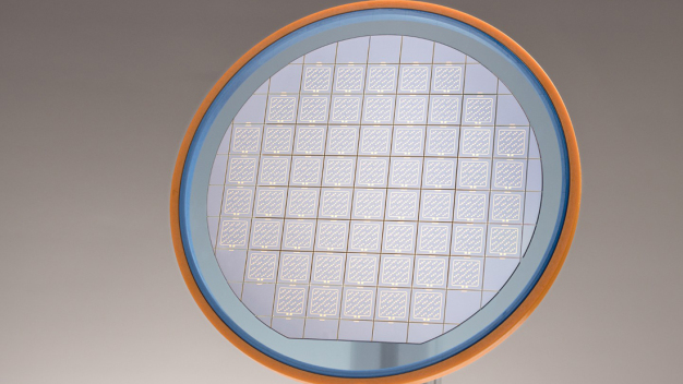
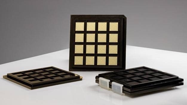
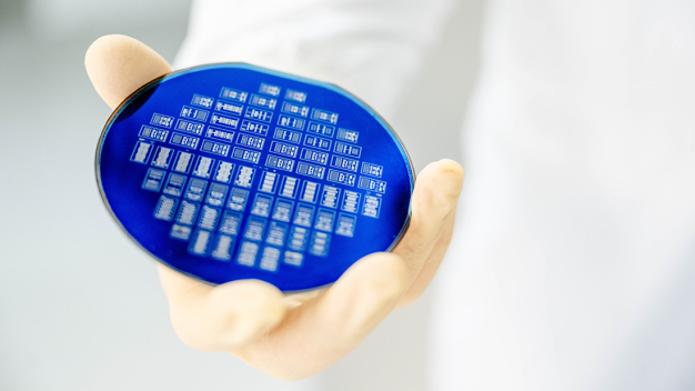
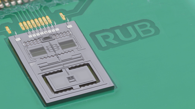
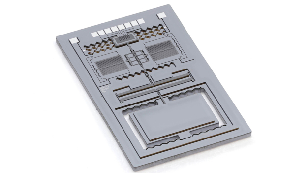
Individual OFET substrates from Fraunhofer IPMS. © Fraunhofer IPMS / Diced OFET substrates from Fraunhofer IPMS. © Fraunhofer IPMS OFET substrate from Fraunhofer IPMS as wafer. © Fraunhofer IPMS / OFET substrates from Fraunhofer IPMS as wafer. © Fraunhofer IPMS OFET substrate from Fraunhofer IPMS in a waffle pack. © Fraunhofer IPMS / OFET substrates from Fraunhofer IPMS in a waffle pack. © Fraunhofer IPMS
  • Electronics (wafers, semiconductors, microchips,...)

Substrates for organic field-effect transistors (OFET) for the development of high-tech materials

Customized silicon chips from Saxony for material characterization of printed electronics

How efficient are new materials? Does changing the properties lead to better conductivity? The Fraunhofer Institute for Photonic Microsystems IPMS develops and manufactures silicon substrates for this purpose. This enables the fundamental electrical characterization of materials such as a novel grap…

  • New building

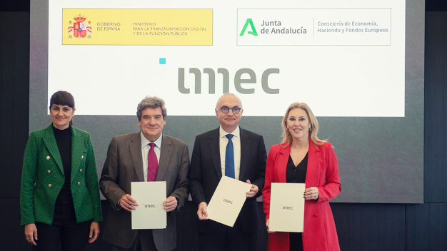
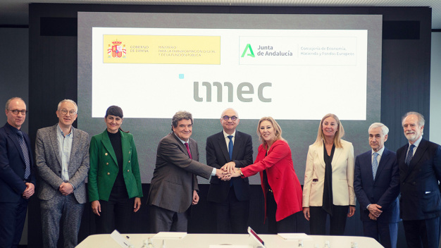
Spanish government, region of Andalusia and imec sign Memorandum of Understanding (MoU) with the intention to establish a new 300mm R&D process line for specialized chip technologies

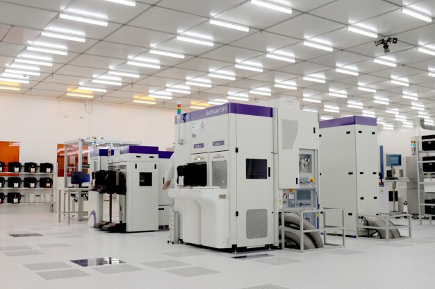
New R&D facility will complement imec’s 300mm cleanroom in Leuven with new processes and materials to boost innovation in upcoming domains such as health and augmented and virtual reality.

The Spanish government, together with the regional government of Andalusia and imec, a world-leading research an…

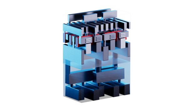
The design pathfinding PDK enables digital designs with 2nm Gate All Around (GAA) technology, including backside connectivity. The design pathfinding PDK allows for digital designs with 2nm Gate All Around (GAA) technology including backside connectivity.
  • Electronics (wafers, semiconductors, microchips,...)

The design pathfinding PDK lowers the threshold for academia and industry to access the most advanced semiconductor technologies

Imec Launches the First Design Pathfinding Process Design Kit for N2 Node

At the 2024 IEEE International Solid-State Circuits Conference (ISSCC), imec, a world-leading research and innovation hub in nanoelectronics and digital technologies, launches its open process design kit (PDK) with a concomitant training program offered through EUROPRACTICE. The PDK will enable virt…

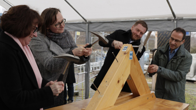
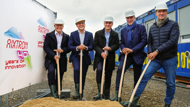
AIXTRON's new Innovation Center Herzogenrath, 23.11.2023: Groundbreaking ceremony for the construction of the new Innovation Center of AIXTRON SE at the Herzogenrath location. From left to right: Dr. Christian Danninger, CFO of AIXTRON SE, Dr. Benjamin Fadavian, Mayor of Herzogenrath, Dr. Felix Grawert, Chairman of the Executive Board & CEO of AIXTRON SE, Kim Schindelhauer, Chairman of the Supervisory Board of AIXTRON SE, Franz-Josef Türuck-Hövener, Technical Deputy Mayor of Herzogenrath. (Photo: AIXTRON/F. Stark)
  • New building

The leading provider of deposition equipment to the semiconductor industry is investing around EUR 100 million at its headquarters in Herzogenrath, Germany. With this, AIXTRON is laying an important foundation for further successful growth.

AIXTRON starts construction of new innovation center

AIXTRON SE (FSE: AIXA, ISIN DE000A0WMPJ6) has officially started the construction of the new innovation center at its headquarters in Herzogenrath, Germany. The leading provider of deposition equipment to the semiconductor industry is investing around EUR 100 million in 1000m2 of clean room with add…

Better informed: With YEARBOOK, NEWSLETTER, NEWSFLASH, NEWSEXTRA and EXPERT DIRECTORY

Stay up to date and subscribe to our monthly eMail-NEWSLETTER and our NEWSFLASH and NEWSEXTRA. Get additional information about what is happening in the world of cleanrooms with our printed YEARBOOK. And find out who the cleanroom EXPERTS are with our directory.

C-Tec Becker Hydroflex ClearClean