and forks (right) with a 20 nm pitch after pattern transfer into a TiN hard mask.")
 process.")
-
- Electronics (wafers, semiconductors, microchips,...)
First electrical tests at 20nm pitch present a next milestone in validating the High NA extreme ultraviolet (EUV) patterning ecosystem
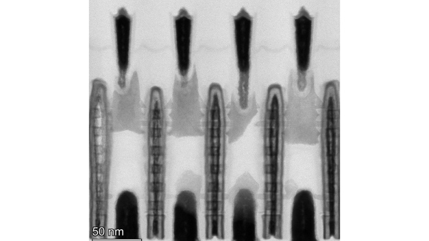
Imec demonstrates electrical yield for 20nm pitch metal lines obtained with High NA EUV single patterning
This week at SPIE Advanced Lithography + Patterning, imec, a world-leading research and innovation hub in nanoelectronics and digital technologies, presents the first electrical test (e-test) results obtained on 20nm pitch metal line structures patterned after single-exposure High NA EUV lithography…


 a single-row CFET and (b) a double-row CFET. The layout of a flip-flop (D-type flip-flop or DFF) shows a reduction of the cell height and area by 24 nm (or 12.5%) when transitioning from a single-row to a double-row CFET (H. Kuekner et al., IEDM 2024).")
. The zoom-in represents a TEM of a monolithic CFET technology demonstrator fabricated within imec’s 300mm R&D cleanroom facility (A. Vandooren et al., IEDM 2024).")

. SEM cross sections are shown along (left) and across (right) the BC/TC.")

.")


 Vision for an optically interconnected multi-XPU computing system at wafer level; and B) demonstrated test system consisting of PIC dies with embedded SiN waveguides (WG) and evanescent couplers, connected to a bottom PIC wafer with complementary SiN evanescent couplers.")

 Schematic cross-section of the chip layer stack, indicating light coupling into the chip, cell illumination, and collection and detection of cell scattering signals. (Right) Experimental scatter plot of a full peripheral blood mononuclear sample measured with the on-chip flow cytometer.")