

New year, new job? View the vacancies! More ...
MT-Messtechnik Pfennig Reinigungstechnik GmbH HJM Berner International GmbH


All publications for the rubric Electronics (wafers, semiconductors, microchips,...)

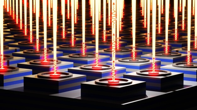
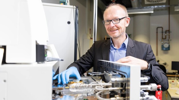
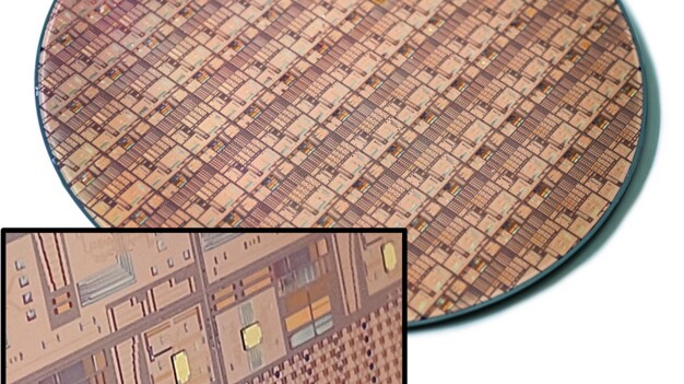
Schematic representation of a scalable platform composed of quantum light sources, where precisely positioned quantum dots are integrated into nanoresonators. Prof. Dr. Reitzenstein in front of the sample chamber of the electron beam lithography system, which produces highly precise nanostructures for scalable next-generation quantum light sources.
  • Know How, Institute

By precisely placed quantum dots, quantum light sources can be integrated onto semiconductor chips in a scalable and reproducible manner for the first time

TU Berlin paves the way for mass production of quantum chips

Optical quantum chips are considered key components of future communication and computer technologies. Their production has so far been complex because the sources needed for individual particles of light – so-called semiconductor quantum dots – formed randomly on the chip and initially had to be lo…

Main entrance at X-FAB's Erfurt site
  • New building

German federal government and Free State of Thuringia support key project for the future of Thuringia’s microelectronics location with Euro 127.4 million

Grant notification presented: X-FAB develops Erfurt site into a center for microsystems technology

A grant notification for Euro 127.4 million was presented today in Erfurt to X-FAB MEMS Foundry GmbH by Thuringia’s Minister President Mario Voigt, Thuringia’s Minister of Economic Affairs Colette Boos-John, and Erfurt’s Mayor Andreas Horn. The funding provided by the German federal government and t…

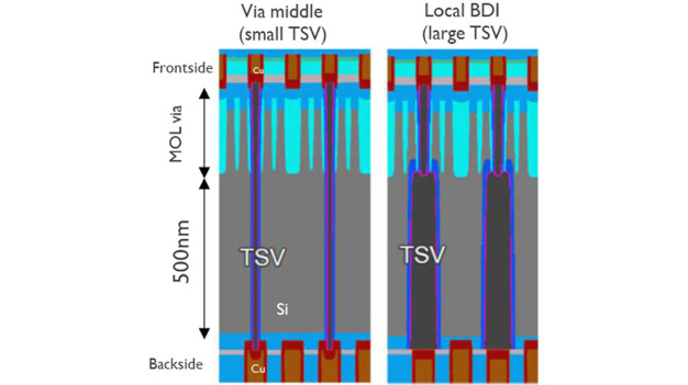
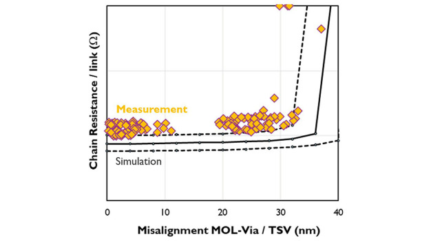
Figure 1 – Schematic comparison of (left) conventional via-middle and (right) local-BDI TSV approaches, assuming a cell height of 115nm and bulk Si thickness of 500nm. Figure 2 – Overlay dependence of the chain resistance of TSV/MOL-via structures, showing 30nm overlay window. The solid black line represents simulations; dashed lines represent ±5% CD.
  • Electronics (wafers, semiconductors, microchips,...)

The new integration approach implements sub-100nm self-aligned through-Si via connections, enabling low-resistance and low-leakage front-to-back connections with good overlay performance.

Sony and imec unveil high-density backside connectivity module enabling next-generation 3D chip integration

– Sony and imec introduce a novel module for integrating highly dense backside sub-100nm through-Si vias (TSVs), based on a self-aligned local backside dielectric isolation (local BDI) step.
– The resulting front-to-back TSVs have lower aspect ratio, 3x lower resistance, 3x larger overlay window, and…

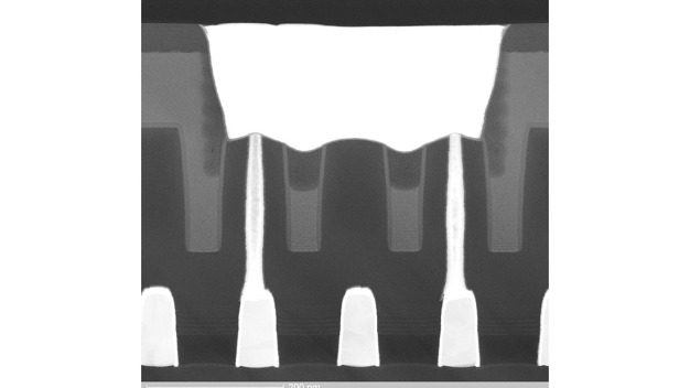
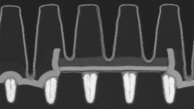
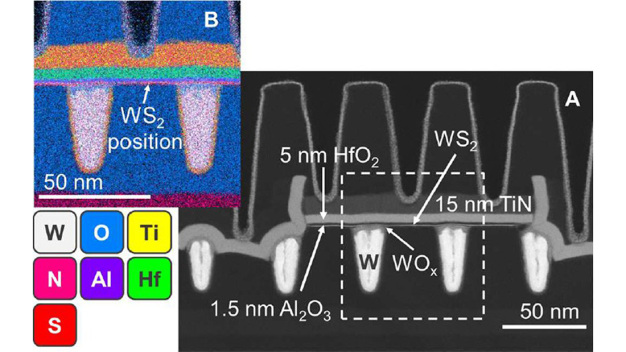
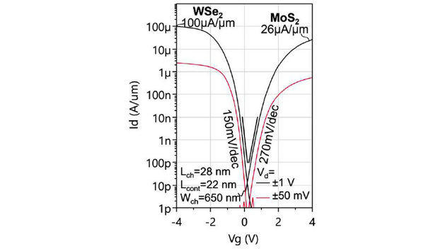
Figure 1 - (A) X-cut HAADF STEM for a WS2 device with a CPP of 50nm, a contact length of 19nm and width of 256nm, after gate connection line etch. And (B) corresponding energy dispersive X-ray spectroscopy (EDS) EDS analysis. Figure 2 – MoS2 nFETs and WSe2 pFETs with 50nm contact pitch and relaxed channel width (650nm), integrated on the same 300mm wafer, show proper threshold voltage matching.
  • Electronics (wafers, semiconductors, microchips,...)

Novel 300mm integration approach for 2D-material based devices enables scaled n and pFETs with 50nm contacted poly pitch.

ASML, TSMC and imec bring industry-ready 2D-material transistors closer with breakthrough 300mm integration

– ASML, TSMC, and imec introduce an innovative 300-mm integration process for transistors based on 2D materials, enabling the first scalable n- and p-FETs with a contact pitch (CPP) of 50 nm, structured using EUV lithography.
– Good results were achieved with scaled nFETs (with MoS2 channel) and pFET…

High-density MIMCAP in a 300mm silicon interposer High-density MIMCAP in a 300mm silicon interposer
  • Electronics (wafers, semiconductors, microchips,...)

Imec unlocks system-level III-V chiplet integration on Si-CMOS by advancing its 300mm RF silicon interposer platform with high-density MIMCAPs, passive modeling, and laser-assisted bonding

– Imec is evolving its 300mm RF silicon interposer into a unique, system-level platform for the heterogeneous integration of III‑V chiplets on Si‑CMOS – targeting mmWave/sub‑THz wireless and high‑speed data center applications.
– A new MIMCAP architecture delivers a 10-to-100-fold increase in capacit…

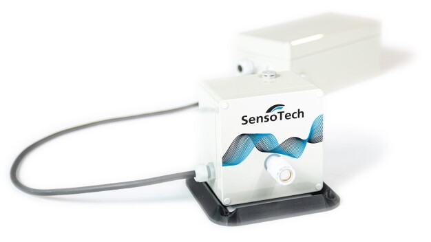
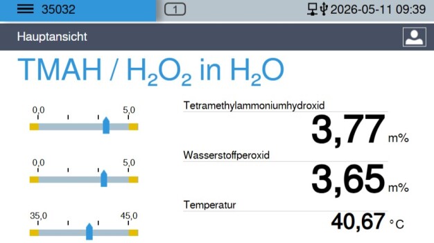
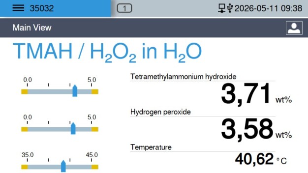
The new SensoTech sensor enables continuous inline monitoring of chemical concentrations in semiconductor wet processes. (Image: SensoTech GmbH) The controller visualizes the inline-measured concentrations of, for example TMAH and H₂O₂ as well as the process temperature, in real time. (Image: SensoTech GmbH) The controller visualizes the inline-measured concentrations of, for example TMAH and H₂O₂ as well as the process temperature, in real time. (Image: SensoTech GmbH)
  • Electronics (wafers, semiconductors, microchips,...)

Measure concentrations inline in processes such as SC1, SC2 and BOE

New ultrasonic sensor from SensoTech for semiconductor wet processes

New sensor technology measures critical chemicals directly in the running process and helps semiconductor manufacturers detect process deviations earlier, reduce (lab) effort and run wet processes more stably.

In semiconductor manufacturing, reliable, controlled wet processes determine yield, quality…

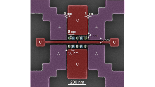
Functioning array of qubits with gaps between plunger (P) and barrier (B) gates of barely 6 nanometers, enabled by High NA EUV lithography. The image also shows the accumulation gates (A) and confinement (C).
  • Electronics (wafers, semiconductors, microchips,...)

The most advanced lithography system, crucial for future advanced memory and computer chips, will play a key role in scaling up quantum technology.

World first: imec presents quantum dot qubit device using High NA EUV lithography

    1. Imec presents a world first: a quantum dot qubit device fabricated using High NA EUV lithography.   
2. This demonstration marks a milestone toward the industrial scaling of more reliable qubits, the basic computational units of quantum computers. Quantum computers will perform exponentially bette…

Better informed: With YEARBOOK, NEWSLETTER, NEWSFLASH, NEWSEXTRA and EXPERT DIRECTORY

Stay up to date and subscribe to our monthly eMail-NEWSLETTER and our NEWSFLASH and NEWSEXTRA. Get additional information about what is happening in the world of cleanrooms with our printed YEARBOOK. And find out who the cleanroom EXPERTS are with our directory.

Hydroflex C-Tec Piepenbrock ClearClean