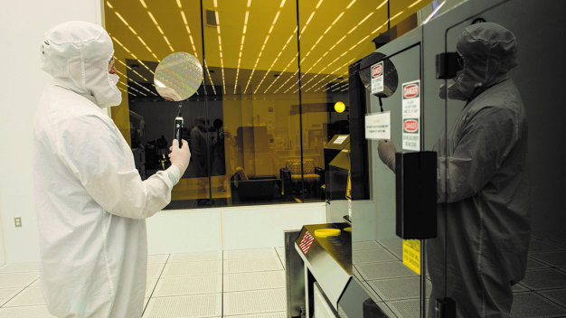
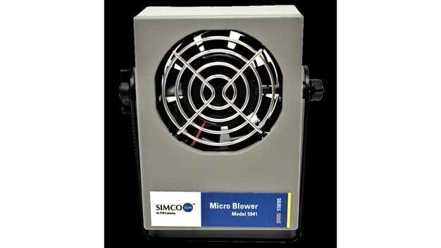
New year, new job? View the vacancies! More ...
PMS Buchta Pfennig Reinigungstechnik GmbH Becker


All publications for the rubric Electronics (wafers, semiconductors, microchips,...)

eBeam metrology equipment from Applied Materials in the cleanroom of Fraunhofer IPMS. © Fraunhofer IPMS / Applied Materials' eBeam metrology equipment at cleanroom of Fraunhofer IPMS. © Fraunhofer IPMS
  • Electronics (wafers, semiconductors, microchips,...)

Launch of European Semiconductor- Metrology Technology Hub

Applied Materials and Fraunhofer IPMS launch European Semiconductor- Metrology Technology Hub

– New hub will provide state-of-the-art metrology systems to accelerate semiconductor research and enhance development projects with chipmakers and ecosystem partners across Europe, particularly in ICAPS* market segments
– Collaboration to accelerate learning, develop novel methods and prove new me…

  • Electronics (wafers, semiconductors, microchips,...)

ASML is making a substantial commitment in imec's future state-of-the-art pilot line

Imec and ASML sign Memorandum of Understanding (MoU) to support semiconductor research and sustainable innovation in Europe

Imec, a leading research and innovation hub in nanoelectronics and digital technologies, and ASML Holding N.V. (ASML), a leading supplier to the semiconductor industry, today announce that they intend to intensify their collaboration in the next phase of developing a state-of-the-art high-numerical…

  • Electronics (wafers, semiconductors, microchips,...)

Merck and Intel Accelerate Sustainable Semiconductor Processes and Manufacturing Technologies Through Academic Research in Europe

– Collaborative research program to harness and augment state-of-the-art artificial intelligence
– Aiming for breakthroughs in more sustainable semiconductor processes and manufacturing technologies

Merck, a leading science and technology company, and Intel Corporation, one of the world’s largest semi…

Electrical engineering student Matthias Wagner immerses the silicon wafer into a development bath in the cleanroom. Microscopic image of perhaps the smallest university logo in the world: The line width is 8 µm, the logo is approximately 50 µm wide ... ... , so this is at least the smallest HKA logo in the world.
  • Electronics (wafers, semiconductors, microchips,...)

Electrical engineering student at Hochschule Karlsruhe creates a three-dimensional HKA logo with line thickness of one-tenth of a hair's width

Maybe the smallest university logo in the world?

A very special semester project was chosen by Matthias Wagner: he created the smallest HKA logo in the world as a three-dimensional microstructure. The structure consists of a plastic-like polymer and is applied to a silicon substrate. The letters of the logo have a line thickness of only about 8 µ…

Better informed: With YEARBOOK, NEWSLETTER, NEWSFLASH, NEWSEXTRA and EXPERT DIRECTORY

Stay up to date and subscribe to our monthly eMail-NEWSLETTER and our NEWSFLASH and NEWSEXTRA. Get additional information about what is happening in the world of cleanrooms with our printed YEARBOOK. And find out who the cleanroom EXPERTS are with our directory.

Systec & Solutions GmbH MT-Messtechnik HJM Vaisala