




- Science
- Translated with AI
3D detector for neutrino research
Microchips with depth structures are designed to distinguish particles by their angle of incidence.
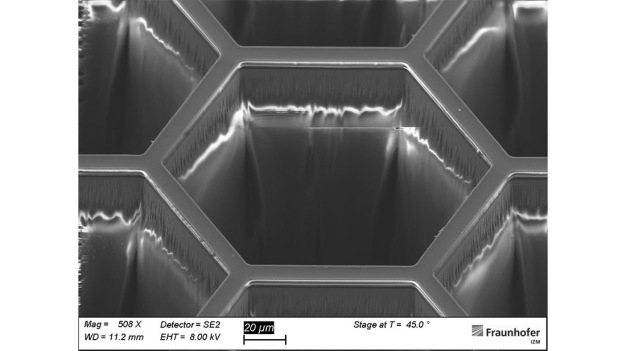
Honeycombs at the micrometer scale: Using an optimized deep-etching process, researchers at Fraunhofer IZM created 3D structures around 250 micrometers deep in a silicon detector. The active sidewalls are intended to detect electrons depending on their angle of incidence. © Fraunhofer IZM
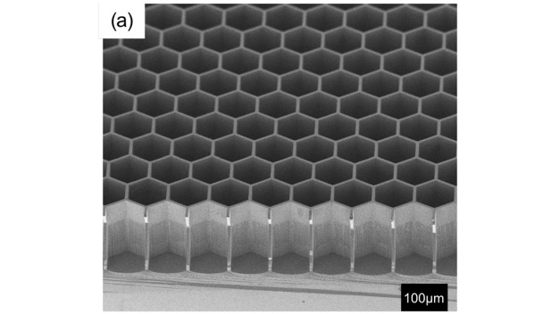
(a) Top view of the array of hexagonal cavities forming a regular honeycomb structure in the silicon. The dark areas correspond to the etched cavities, while the bright lines represent the remaining silicon strut network between the cells.
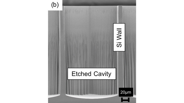
(b) Overview image of the hexagonal cavity in cross section; the dark gray area corresponds to the remaining silicon, and the light area to the etched cavity (“Etched Cavity”).
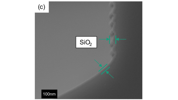
(c) Cross-section after SiO₂ deposition; the light-gray layer contrasting with the dark-gray Si substrate is the deposited SiO₂ on the sidewall and cavity floor.
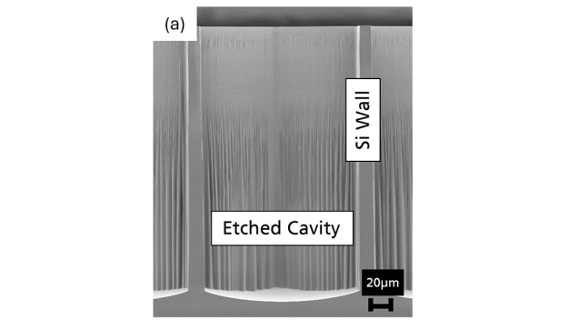
(a) Overview image of the hexagonal cavity in cross-section (Cross Section); the dark gray area corresponds to the remaining silicon, while the light area represents the etched cavity (“Etched Cavity”).
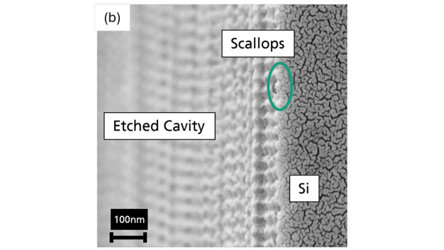
(b) Detailed view of the sidewall at high magnification; the periodic bulges (“scallops”) of the Bosch process are clearly visible and serve to assess the sidewall roughness.
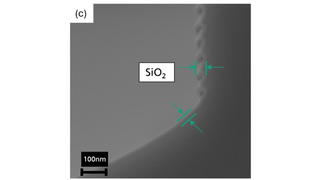
(c) Cross-section after SiO₂ deposition; the light gray layer contrasting with the dark gray Si substrate is the deposited SiO₂ on the sidewall and cavity bottom.
Fraunhofer researchers, together with the University of Münster, have developed a wafer-based manufacturing process for a novel silicon diode that measures particles depending on their angle of incidence. In the future, the energy-filter diode is intended to help distinguish between signal and background electrons that hit a detector with nearly identical energies but different angles of incidence. One possible application is the international KATRIN experiment for determining the neutrino mass. In the cleanroom of Fraunhofer IZM, deep, honeycomb-shaped microstructures were introduced into large-area detector wafers, electrically passivated, and transferred to the University of Münster for further investigations.
The KATRIN experiment investigates the electron spectrum of tritium beta decay near its endpoint energy of 18.57 kiloelectronvolts. This makes it possible to draw conclusions about the mass of the neutrino. The measurement is made more difficult by the fact that certain background electrons arrive at the detector with nearly the same kinetic energy as the signal electrons being sought. However, there is a significant difference in their angle of incidence: A large proportion of the background electrons reach the detector at angles typically below ten degrees, while signal electrons can have angles of up to approximately 50 degrees.
Conventional detectors do not provide suitable angular information at low particle energies, in strong magnetic fields, and under ultrahigh-vacuum conditions. This is precisely where the active transverse energy filter comes in. Deep, hexagonal recesses are etched into the surface of a Si-PIN diode. Electrons with a larger angle of incidence are more likely to hit the active sidewalls of the honeycomb structure and generate a measurable signal there. Electrons with small angles, by contrast, predominantly reach the inactive bottom of the structure. Previous investigations on small-format prototypes at the University of Münster have already demonstrated angle-dependent detection efficiency. Simulations also show that a structure optimized for the KATRIN experiment could reduce the electron background by a factor of three to five. This estimate depends on the composition of the background.
Fraunhofer IZM transfers the concept to wafer scale
The central task of the Fraunhofer Institute for Reliability and Microintegration IZM was to transfer the physical principle into a reproducible, wafer-compatible manufacturing process. The starting point was large-area Si-PIN detector wafers with an unusual 24-sided geometry. Since this special format could not be processed directly with all the equipment in the 200-millimeter cleanroom, the experts developed a temporary carrier concept: The detector wafers were bonded to 200-millimeter silicon wafers using wax and then structured together.
Since only two detector wafers were available, the complete process sequence was first developed on specially manufactured test wafers. This included lithography, deep reactive ion etching, the removal of process residues, detachment from the carrier wafer, and passivation of the resulting sidewalls. Only after the individual steps had been evaluated and optimized was the process transferred to the actual detectors.
250-micrometer-deep honeycomb structures in silicon
A particular challenge was producing nearly vertical, low-defect sidewalls at a target depth of around 250 micrometers. For the lithography, the researchers selected a positive resist that provided nearly vertical flanks and sufficient resistance for the subsequent deep etching process. To transfer the honeycomb-shaped mask structure into the silicon as precisely as possible, the special exposure conditions of the detector wafer, which was elevated on the carrier, also had to be taken into account.
For deep reactive ion etching, or DRIE, the team at Fraunhofer IZM developed a cyclic process consisting of passivation, anisotropic etching, and isotropic etching. Using a statistical design of experiments, five process parameters were systematically varied. These included process pressure, plasma power, gas flow, and wafer temperature. The results showed a significant correlation between wafer temperature and the formation of unwanted silicon structures, known as “silicon grass.” By adjusting the process parameters, the researchers succeeded in identifying a process window for largely vertical sidewalls with minimized defects.
Passivation protects the sensitive sidewalls
After etching, the sidewalls were passivated with silicon dioxide. This insulating layer is intended to saturate surface states, limit charging effects, and reduce surface-related dark currents. Thermal oxidation was not an option because of the existing metallization and the limited thermal budget of the detector wafers. The team therefore used plasma-enhanced chemical vapor deposition (PECVD) at 175 degrees Celsius.
With deep structures, achieving uniform coating of the upper, middle, and lower sidewall areas is particularly challenging. By adjusting the PECVD process, the team achieved improved layer coverage. Thicknesses of 161 nanometers in the upper, 80 nanometers in the middle, and 55 nanometers in the lower sidewall area were measured. The process could be combined with the already metallized Si-PIN diodes.
In several design stages, the researchers at Fraunhofer IZM produced initial detector wafers, which are now being used for test measurements at the University of Münster.
Technological basis for novel particle detectors
By developing the complete process sequence, Fraunhofer IZM has created a technological basis for three-dimensional, angle-dependent silicon detectors. The work combines application-oriented nanofabrication with the requirements of experimental particle physics. Particularly valuable are not only the successfully established lithography, DRIE, and PECVD processes, but also the insights gained into the interaction between microgeometry, semiconductor layer structure, and signal measurement.
The 3D energy-filter diode is therefore not yet a ready-to-use detector. However, the manufacturing technology developed and the insights gained from the first demonstrator provide a solid foundation for further refining the device architecture and experimentally exploring the potential of angle-dependent particle detection.
Fraunhofer-Institut für Zuverlässigkeit und Mikrointegration IZM
13355 Berlin
Germany