


New year, new job? View the vacancies! More ...
Buchta PMS C-Tec ClearClean


All publications for the rubric Electronics (wafers, semiconductors, microchips,...)

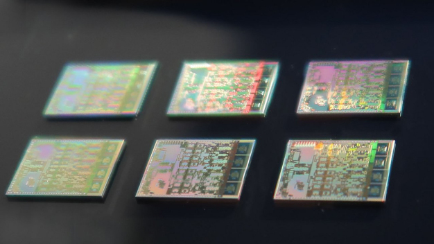
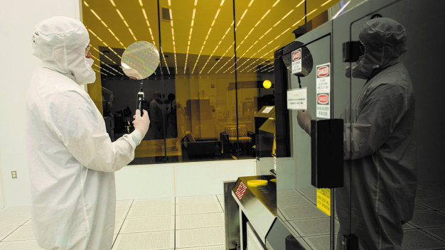
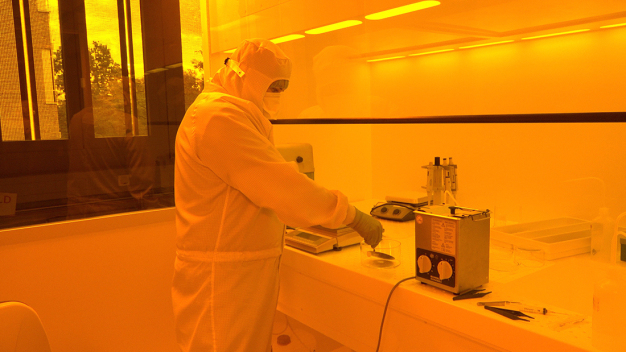
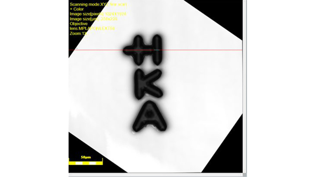
Electrical engineering student Matthias Wagner immerses the silicon wafer into a development bath in the cleanroom. Microscopic image of perhaps the smallest university logo in the world: The line width is 8 µm, the logo is approximately 50 µm wide ... ... , so this is at least the smallest HKA logo in the world.
  • Electronics (wafers, semiconductors, microchips,...)

Electrical engineering student at Hochschule Karlsruhe creates a three-dimensional HKA logo with line thickness of one-tenth of a hair's width

Maybe the smallest university logo in the world?

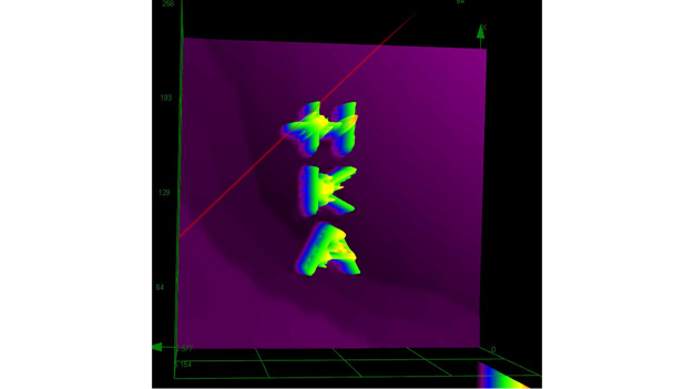
A very special semester project was chosen by Matthias Wagner: he created the smallest HKA logo in the world as a three-dimensional microstructure. The structure consists of a plastic-like polymer and is applied to a silicon substrate. The letters of the logo have a line thickness of only about 8 µm…

(Copyright: I'm Thongchai - stock.adobe.com)
  • Electronics (wafers, semiconductors, microchips,...)

Multi-year framework agreement for semiconductor equipment in the upper double-digit million euro range concluded at the end of 2022.

Major order in the field of semiconductor equipment

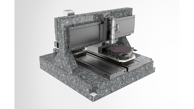
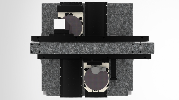
The Jenoptik photonics group concluded a framework agreement with a global technology group at the end of 2022 with a total volume in the upper double-digit million euro range and a term of three years. The contract covers the manufacture of complex micro-optical components used in semiconductor pro…

Better informed: With YEARBOOK, NEWSLETTER, NEWSFLASH, NEWSEXTRA and EXPERT DIRECTORY

Stay up to date and subscribe to our monthly eMail-NEWSLETTER and our NEWSFLASH and NEWSEXTRA. Get additional information about what is happening in the world of cleanrooms with our printed YEARBOOK. And find out who the cleanroom EXPERTS are with our directory.

Vaisala Becker MT-Messtechnik Systec & Solutions GmbH