- Science
Chemnitz becomes a European hub for semiconductor testing and reliability research with the new "European Test and Reliability Center"
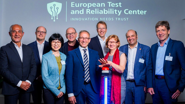
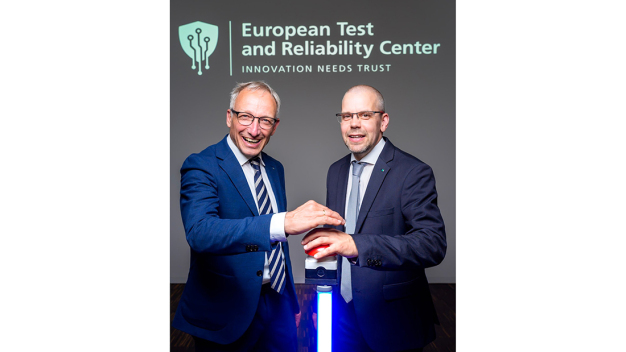
Fraunhofer ENAS celebrates the opening of the “European Test and Reliability Center” (ETRC). With support from the European Union (EU), the Federal Ministry of Research, Technology and Space (BMFTR) and the Free State of Saxony, the Fraunhofer Institute for Electronic Nano Systems ENAS is establishing a new European center for testing and reliability assessment of complex semiconductor components in Chemnitz.
The Fraunhofer Institute for Electronic Nano Systems ENAS in Chemnitz has reached an important milestone with the opening of its “European Test and Reliability Center” (ETRC). The newly established competence center in Chemnitz brings together strategic expertise in testing and reliability assessments of semiconductor components, thereby strengthening Saxony's role as a high-tech location in the European semiconductor ecosystem.
The goal of the new center is to establish an industry- and application-oriented infrastructure for new testing strategies and reliability routines for semiconductor technologies that meet the increasing demands of modern microelectronics. To this end, the ETRC is receiving several million euros in funding from the EU through the European Regional Development Fund (ERDF) and the Just Transition Fund (JTF), as well as from the Free State of Saxony. Further expansion of research and development capacities will take place within the framework of the pilot line for “Advanced Packaging and Heterogeneous Integration for Electronic Components and Systems” (APECS), for which additional funding is being provided by the EU, BMFTR, and the state of Saxony. APECS is a central component of the European Chips Act, coordinated by the Fraunhofer-Gesellschaft and implemented by the Research Fab Microelectronics Germany (FMD).
The ETRC is a strategic platform for the development, testing, and validation of innovative testing and reliability methods along the entire semiconductor value chain, from chip design to front-end and packaging. The focus is on new key technologies such as wide-bandgap semiconductors (e.g., silicon carbide and gallium nitride), modular chip architectures (chiplets), microsystems (MEMS), and photonic-electronic co-designs, all of which will ensure quality, functionality, robustness, and longevity in Europe in the future. The ETRC develops customized testing strategies for this purpose and provides an application-oriented environment in which chips, modules, and complete systems are tested under real-world conditions.
With AI-supported fault analysis, thermal-electrical stress simulation, and a modern test data infrastructure, the ETRC can support companies and research institutions in achieving series production of new semiconductor products faster, more reliably, and more sustainably. Particularly in safety-critical applications, such as in the automotive industry, medical technology, or the Industrial Internet of Things, the ability to test components for fault tolerance and system behavior at an early stage is a strategic competitive advantage.
The ETRC also acts as a transfer and collaboration platform. It provides OEMs, suppliers, small and medium-sized enterprises (SMEs), as well as research institutions a shared space to develop new testing standards and bring technologies to market maturity together. For SMEs, low-threshold access to high-end test infrastructure via shared facilities is an important lever for democratizing innovation and thus strengthening European SMEs in the long term.
By systematically building up independent testing and reliability expertise at its Chemnitz site, the ETRC is helping to close an important gap in the European semiconductor ecosystem. While the manufacture and design of semiconductors have received increased support from political funding programs in recent years, there has been a lack of neutral, industry-ready testing and verification platforms to accompany developments from the initial idea to series production. In addition, the majority of semiconductor testing has taken place outside Europe, which is associated with long delivery times and geopolitical uncertainties. The establishment of the ETRC as Europe's new competence center for testing and reliability creates a modern testing environment in the heart of Saxony that makes semiconductor products more reliable right from the development stage, accelerates innovation, and ensures quality from the outset.
Prof. Dr. Harald Kuhn, Director of Fraunhofer ENAS, sums up the strategic importance of the new center: "With the ETRC, we are sending a strong signal of Europe's commitment to combining technological excellence with proven quality and reliability. It represents a shift in the innovation process towards a connected, accelerated circular thinking. This is a decisive step towards securing quality, sustainability, and economic independence in the semiconductor market in the long term. I am convinced that the ETRC will provide decisive impetus for Europe's technological sovereignty and competitiveness."
With strong links to Chemnitz University of Technology, the Research Fab Microelectronics Germany (FMD), and the European pilot line for “Advanced Packaging and Heterogeneous Integration for Electronic Components and Systems” (APECS), the ETRC represents not only technological excellence but also a new model of European, location-integrated innovation promotion. It is a place where industrial relevance, scientific expertise, and strategic autonomy converge. This strengthens Saxony's role as a key location for the resilient and innovation-driven semiconductor production of tomorrow.
Fraunhofer-Institut für Elektronische Nanosysteme ENAS
09126 Chemnitz
Germany
