Here you can find the NEWSLETTER archive More ...
Becker PMS MT-Messtechnik HJM

cleanroom online
Deutsch   English


All publications from IMEC Belgium

Vertikaler Pufferleckstrom in Durchlassrichtung, gemessen an 1200V GaN-on-QST® bei zwei verschiedenen Temperaturen: (links) 25°C und (rechts) 150°C. Der 1200V-Puffer von Imec zeigt einen vertikalen Leckstrom unter 1µA/mm2 bei 25°C und unter 10µA/mm2 bei 150°C bis zu 1200V mit einem Durchbruch von über 1800V sowohl bei 25°C als auch bei 150°C, was ihn für die Verarbeitung von 1200V-Bauteilen geeignet macht. / Vertical forward buffer leakage current measured on 1200V GaN-on-QST® at two different temperatures: (left) 25°C and (right) 150°C. Imec’s 1200V buffer shows vertical leakage current below 1µA/mm2 at 25°C and below 10µA/mm2 at 150°C up to 1200V with a breakdown in excess of 1800V both at 25°C and 150°C, which makes it suitable for the processing of 1200V devices.

This breakthrough result paves the way for GaN to enter into the SiC high voltage domain

Imec and AIXTRON Demonstrate 200 mm GaN Epitaxy on AIX G5+ C for 1200V Applications with Breakdown in Excess of 1800V

Imec, a world-leading research and innovation hub in nanoelectronics and digital technologies, and AIXTRON, the leading provider of deposition equipment for compound semiconductor materials, have demonstrated epitaxial growth of gallium-nitride (GaN) buffer layers qualified for 1200V applications on…

The Neuropixels 2.0 probe (bottom) is smaller than the first generation (top) and can monitor neural activity over weeks.

A new generation of miniature recording probes can track the same neurons inside tiny mouse brains over weeks — and even months

Latest Neuropixels probes can track neurons over weeks

The new tools build on the success of the original Neuropixels probes released in 2017 and currently used in more than 400 labs. Neuropixels 2.0 are much smaller — about a third the size of their predecessors. They’re designed to record the electrical activity from more individual neurons and ha…

28nm Pitch Single-Exposure-Strukturierung mit dem MOx-Prozess von Inpria auf einem 0,33NA EUV-Vollfeldscanner nach Ru-Metallisierung. / 28nm pitch single-exposure patterning using Inpria’s MOx process on a 0.33NA EUV full field scanner after Ru metallization. 24nm Pitch-Linien/Abstände, erzielt auf einem 0,33NA NXE:3400B Vollfeldscanner, (links) nach dem Entwickeln und (rechts) nach dem Ätzen auf der kritischen Zielgröße (CD) (uLER = unbiased line-edge roughness). / 24nm pitch line/spaces obtained on a 0.33NA NXE:3400B full field scanner, (left) after developing and (right) after etching on target critical dimension (CD) (uLER = unbiased line-edge roughness). 28nm Kontaktlöcher, erzielt mit einem 0,33NA NXE:3400 Vollfeldscanner, nach dem Entwickeln. / 28nm contact holes obtained on a 0.33NA NXE:3400 full field scanner, after developing.

Proven correlation between morphological and electrical data on 28nm pitch line/spaces increases understanding of stochastic defectivity impact on device reliability/yield

Imec Pushes Single-Exposure Patterning Capability of 0.33NA EUVL to its Extreme Limits

This week, at the 2021 SPIE Advanced Lithography Conference, imec, a world-leading research and innovation hub in nanoelectronics and digital technologies, and ASML, the world’s leading manufacturer of semiconductor lithography equipment, present several papers that demonstrate the ultimate single…

Collaboration between Sarcura and imec aims to develop a silicon photonics-based cytometry solution allowing real-time process control and manipulation of cells.

SARCURA and imec to collaborate on high throughput cytometry solution for automated (T-)cell separation, tackling manufacturing challenges of cell and gene therapies

Sarcura GmbH, an Austrian early-stage technology startup, today announced that it has entered a collaboration with imec, a world-leading research and innovation hub in nanoelectronics and digital technologies to develop a silicon chip-based prototype of a cytometer for automated cell separation brin…

SWIR-Bilder für 3 verschiedene Pixelabstände. Die Bilder mit der höchsten Auflösung konnten mit dem kleinsten (1,82 µm) Pixelabstand aufgenommen werden. / SWIR images for 3 different pixel pitches. Highest resolution images could be captured with the smallest (1.82 µm) pixel pitch. Der Dünnfilm-Photodetektor wurde monolithisch auf einer kundenspezifischen Si-CMOS-Ausleseschaltung integriert. (Bildnachweis: Imec) 
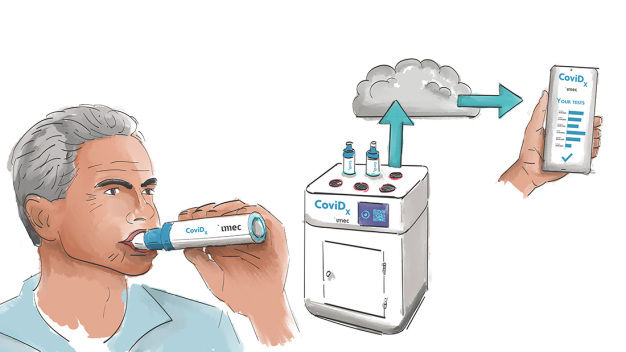
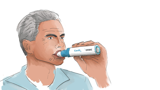
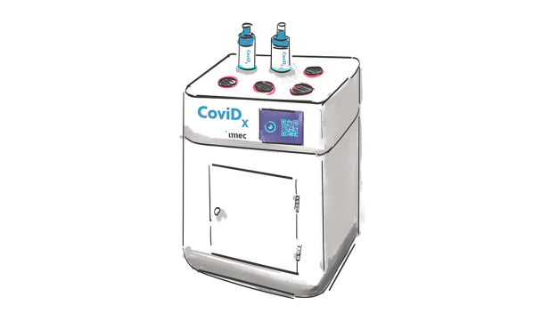
/ The thin-film photodetector was monolithically integrated on a custom Si-CMOS readout circuit. (Source: Imec)

The monolithic integration of the thin-film photodetector with CMOS readout circuitry offers a path to high-throughput wafer-level manufacturing

Imec Presents a Thin-Film Short-Wave-InfraRed Image Sensor with Sub-2µm Pixel Pitch

Imec, a world-leading research and innovation hub in nanoelectronics and digital technologies, presents a prototype high-resolution short-wave-infrared (SWIR) image sensor with record small pixel pitch of 1.82 µm. It is based on a thin-film photodetector that is monolithically integrated on a custo…

Der bahnbrechende Ansatz wird Viruspartikel in ausgeatmeter Luft für schnelle, einfache, bequeme und groß angelegte Tests verwenden

Imec beginnt mit der Entwicklung eines SARS-CoV-2-Tests, um positive Fälle zu identifizieren und in weniger als fünf Minuten zu bestätigen, ob jemand ansteckend ist

Imec, ein weltweit führendes Forschungs- und Innovationszentrum für Nanoelektronik und digitale Technologien, gab bekannt, dass es mit der Entwicklung eines bahnbrechenden SARS-CoV-2-Tests begonnen hat. Im Gegensatz zu derzeitigen Ansätzen (mit Blut, Speichel oder einem Nasen-Rachen-Abstrich) wir…

Better informed: With YEARBOOK, NEWSLETTER, NEWSFLASH and EXPERT DIRECTORY

Stay up to date and subscribe to our monthly eMail-NEWSLETTER and our NEWSFLASH. Get additional information about what is happening in the world of cleanrooms with our printed YEARBOOK. And find out who the cleanroom EXPERTS are with our directory.

Hydroflex Ecolab Vaisala PPS