


New year, new job? View the vacancies! More ...
Systec & Solutions GmbH PMS HJM Buchta


All publications from IMEC Belgium

Figure 1 – (Left) Transfer curves of 2D-pFET devices using defect-passivated synthetically-created bi-layer WSe2 films, with the best device showing Imax = 690µA/µm; (Right) TEM cross-section of the finalized dual-gated 2D pFET (Lch=channel length; TG=Top Gate; BG=Back Gate; S=Source; D=Drain; IL=Interlayer), in collaboration with TSMC. Figure 2 – (a) Dry etching into SiO₂; (b) Dry and wet etching, which stops selectively on the WS₂ monolayer channel, also removing the AlOx interlayer laterally along the entire channel length (in collaboration with Intel).
  • Electronics (wafers, semiconductors, microchips,...)

Collaboration with leading semiconductor manufacturers pivotal in optimizing the key modules for 2D-material device integration

Imec advances 2D-material based device technology beyond state of the art in support of the future logic technology roadmap

– Imec, in collaboration with leading semiconductor manufacturers, addressed key challenges in advancing 2D-material device technology, which is considered a long-term option for extending the logic technology roadmap.
– Collaboration with TSMC resulted in record performing WSe2 -based pFETs (with Im…

Imec pioneers full wafer-scale (300mm) production of solid-state nanopores with EUV lithography, as shown in the photo. © imec Cross-sectional and top-view TEM of the fabricated solid-state nanopore. Cross-sectional and top-view TEM of the fabricated solid-state nanopore.
  • Electronics (wafers, semiconductors, microchips,...)

Breakthrough enables scalable, high-precision biosensing applications in life sciences and healthcare

Imec demonstrates first wafer-scale fabrication of solid-state nanopores using EUV lithography

1. Imec has achieved the first successful wafer-scale fabrication of solid-state nanopores using EUV lithography on 300mm wafers. This innovation transforms nanopore technology from a lab-scale concept into a scalable platform for biosensing, genomics and proteomics.
2. Nanopores are hailed as gamech…

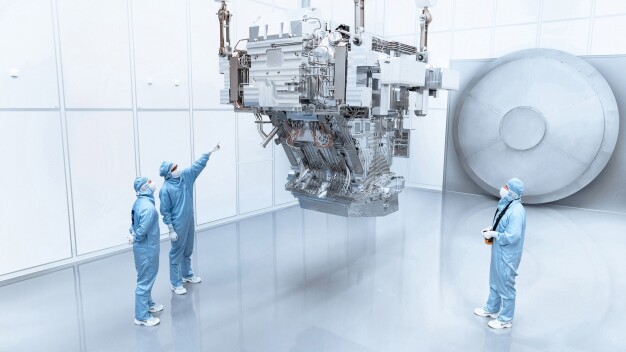
The cleanroom at Imec forms the basis for NanoIC's PDKs, which are based on 2-nm process flows.
  • Workshop / Course

Major update of NanoIC’s Pathfinding N2 P-PDK empowers researchers and designers to learn and innovate on full SoC architectures.

NanoIC adds advanced SRAM memory macros to its N2 pathfinding PDK

This week, at SEMICON Europe, the NanoIC pilot line, a European initiative coordinated by imec and dedicated to accelerating innovation in chip technologies beyond 2nm, announces the release of the N2 P-PDK v1.0, an important update of its N2 Pathfinding Process Design Kit (P-PDK). This new version…

Links: current CEO, Luc Van den hove, Right: imec CEO as of April 1, 2026, Patrick Vandenameele. CEO of imec starting April 1, 2026, Patrick Vandenameele.
  • Company

Imec Ensures Seamless Succession and Strategic Continuity

Leadership Transition at imec: Luc Van den hove Becomes Chairman, Patrick Vandenameele Appointed as Next CEO of imec

The Board of Directors of imec, a world-leading research and innovation hub in nanoelectronics and digital technologies, has appointed Patrick Vandenameele as the next Chief Executive Officer. Effective April 1, 2026, he will succeed current CEO Luc Van den hove, who will then assume the role of Cha…

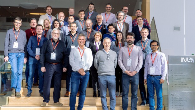
Representatives of the twelve consortium members gathered at the International Iberian Nanotechnology Laboratory in Braga, Portugal.
  • Electronics (wafers, semiconductors, microchips,...)

Consortium to facilitate access to design infrastructure, training, and capital for European fabless semiconductor startups, small and medium enterprises and research organizations.

Imec coordinates EU Chips Design Platform

A consortium of 12 European partners, coordinated by imec, has been selected in the framework of the European Chips Act to develop the EU Chips Design Platform. Funded by Chips JU, the platform will facilitate access to advanced semiconductor design infrastructure, training, and capital for fabless…

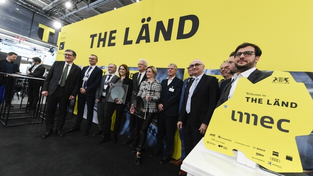
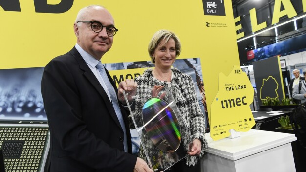
Luc Van de Hofe and Nicole Hoffmeister-Kraut
  • Electronics (wafers, semiconductors, microchips,...)

New partnership enables an innovative network together with academia and industry partners to strengthen digital sovereignty in Europe

Baden-Württemberg attracts imec to lead development of chiplet-based technology for automotive applications

Imec, a world-leading research and innovation hub in nanoelectronics and digital technologies, and the State Government of Baden-Württemberg, Germany, today announced, at the Hannover Trade Fair, the launch of the Advanced Chip Design Accelerator (ACDA). The new imec competence center in Baden-Württ…

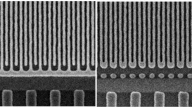
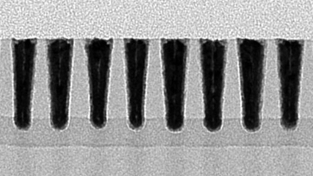
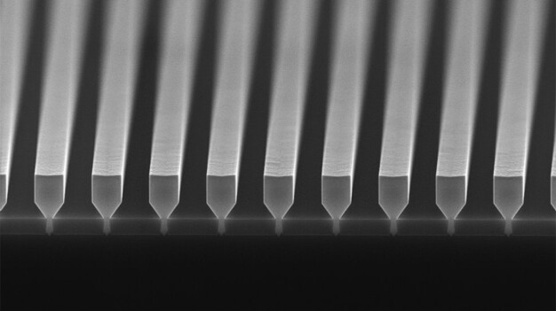
Figure 1 – Top-down SEM images of meanders (left) and forks (right) with a 20 nm pitch after pattern transfer into a TiN hard mask. Figure 2 – TEM image of metallized wires with a 20 nm pitch after a chemical-mechanical polishing (CMP) process.
  • Electronics (wafers, semiconductors, microchips,...)

First electrical tests at 20nm pitch present a next milestone in validating the High NA extreme ultraviolet (EUV) patterning ecosystem

Imec demonstrates electrical yield for 20nm pitch metal lines obtained with High NA EUV single patterning

This week at SPIE Advanced Lithography + Patterning, imec, a world-leading research and innovation hub in nanoelectronics and digital technologies, presents the first electrical test (e-test) results obtained on 20nm pitch metal line structures patterned after single-exposure High NA EUV lithography…

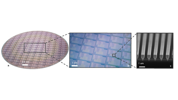
A 300 mm silicon wafer containing thousands of GaAs devices with a close-up of multiple dies and a scanning electron micrograph of a GaAs nano-ridge array after epitaxy. A 300 mm silicon wafer containing thousands of GaAs devices with a close-up of multiple dies and a scanning electron micrograph of a GaAs nano-ridge array after epitaxy.
  • Electronics (wafers, semiconductors, microchips,...)

Imec achieves breakthrough in silicon photonics, paving the way for cost-effective and high-performance optical devices.

First full wafer-scale fabrication of electrically-pumped GaAs-based nano-ridge lasers on 300 mm silicon wafers

Imec, a world-leading research and innovation hub in nanoelectronics and digital technologies, has announced a significant milestone in silicon photonics with the successful demonstration of electrically-driven GaAs-based multi-quantum-well nano-ridge laser diodes fully, monolithically fabricated on…

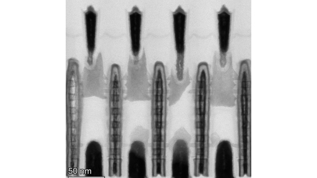
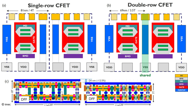
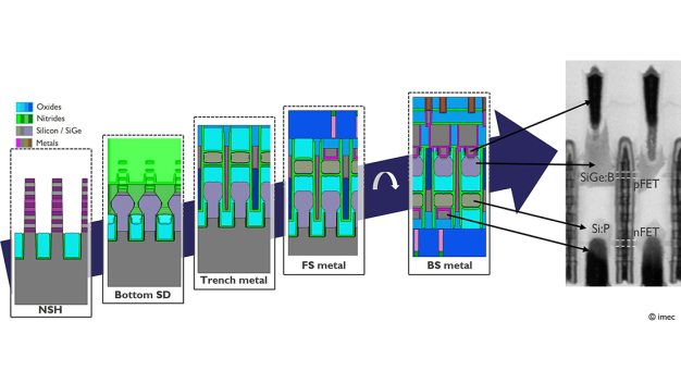
Figure 1 – Conceptual representation of (a) a single-row CFET and (b) a double-row CFET. The layout of a flip-flop (D-type flip-flop or DFF) shows a reduction of the cell height and area by 24 nm (or 12.5%) when transitioning from a single-row to a double-row CFET (H. Kuekner et al., IEDM 2024). Figure 2 – Virtual process flow for building a double-row CFET architecture. The process flow, simulated with 3D Coventor, started from the specifications of a ‘virtual’ CFET fab, projecting future processing capabilities and design margins (H. Kuekner et al., IEDM 2024). The zoom-in represents a TEM of a monolithic CFET technology demonstrator fabricated within imec’s 300mm R&D cleanroom facility (A. Vandooren et al., IEDM 2024).
  • Electronics (wafers, semiconductors, microchips,...)

New standard cell architecture offers the most optimal trade-off between area efficiency and process complexity for logic and SRAM

Imec proposes double-row CFET for the A7 technology node

At the 2024 IEEE International Electron Devices Meeting (IEDM), imec, a world-leading research and innovation hub in nanoelectronics and digital technologies, presents a new CFET-based standard cell architecture containing two rows of CFETs with a shared signal routing wall in between. The main bene…

Better informed: With YEARBOOK, NEWSLETTER, NEWSFLASH, NEWSEXTRA and EXPERT DIRECTORY

Stay up to date and subscribe to our monthly eMail-NEWSLETTER and our NEWSFLASH and NEWSEXTRA. Get additional information about what is happening in the world of cleanrooms with our printed YEARBOOK. And find out who the cleanroom EXPERTS are with our directory.

ClearClean Piepenbrock C-Tec Vaisala