nahm gemeinsam mit Werksleiter Byoung-Hong Lee (links) und Manager Dong-Chul Park (rechts) den Preis entgegen. / As a winner this year, Engel was the first non-Korean company to be presented with the National Quality Award. Robert Bodingbauer, Engel Machinery Korea's president (centre), accepted the award together with plant manager Lee Byoung-Hong (left) and manager Park Dong-Chul (right).")
Engel Machinery Korea receives Presidential National Quality Award
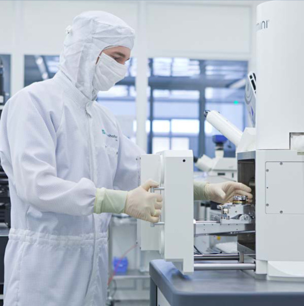
The Korea National Quality Award is one of Korea's most prestigious business awards and one of the most important quality distinctions in the world. At the end of November ENGEL MACHINERY KOREA won this presidential quality award in the field of production innovation. Furthermore, Engel is the first…


 / Figure 3. Typical liquid cycle chamber pressure at 121 °C (250 °F)")
 / Figure 4. Typical prevacuum cycle chamber pressure at 121 °C (250 °F)")
 / Figure 5. Self-Contained Biological Indicators (SCBI)")


")
")
")
")
")