


- Universities
Breaking GaN
Precise instruments for the next generation of LED chips
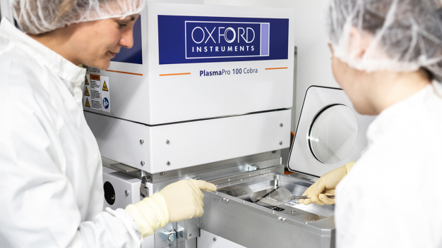
 im neu ausgestatteten Reinraum des Instituts für Halbleitertechnik. (Bildnachweis: Max Fuhrmann/TU Braunschweig) / Dr Jana Hartmann and Juliane Breitfelder (from left) in the newly equipped cleanroom of the Institute of Semiconductor Technology. (Picture Credits: Max Fuhrmann/TU Braunschweig)")
Dr. Jana Hartmann und Juliane Breitfelder (v.l.) im neu ausgestatteten Reinraum des Instituts für Halbleitertechnik. (Bildnachweis: Max Fuhrmann/TU Braunschweig) / Dr Jana Hartmann and Juliane Breitfelder (from left) in the newly equipped cleanroom of the Institute of Semiconductor Technology. (Picture Credits: Max Fuhrmann/TU Braunschweig)
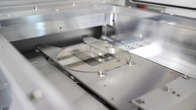
 / While one of the devices is etching, this PECVD unit is depositing new semiconductor layers on the institute’s wafers. (Picture Credits: Max Fuhrmann/TU Braunschweig)")
Während die eine Anlage ätzt, bringt diese PECVD neue Halbleiterschichten auf die Wafer des Instituts. (Bildnachweis: Max Fuhrmann/TU Braunschweig) / While one of the devices is etching, this PECVD unit is depositing new semiconductor layers on the institute’s wafers. (Picture Credits: Max Fuhrmann/TU Braunschweig)
The path to new LED technologies is taken layer by layer and flooded with acid. Highly specialized cleanroom equipment is therefore needed to produce for example blue LEDs from gallium nitride (GaN) at the Institute of Semiconductor Technology. Two new large-scale instruments now open up further avenues for semiconductor technology, from which alliances such as the Cluster of Excellence QuantumFrontiers and the Quantum Valley Lower Saxony (QVLS) benefit in particular. Several years of work are behind this. After all, each of the devices has its own peculiarities that only an electron microscope can uncover.
The installation of the two new large-scale instruments alone – Oxford Plasma Pro 100 and Plasma Pro 80 – is cost-intensive. They need new gas connections, pressure reducers, safety technology and much more. Together with the price of the devices, this adds up to almost one million euros, financed by the QuantumFrontiers cluster, the DFG, and the Institute of Semiconductor Technology at TU Braunschweig. But what do these devices actually do? The question is best asked of Dr. Jana Hartmann. As a junior research group leader, she coordinates the work on the new stars in the institute’s cleanroom.
Dr. Jana Hartmann: “The Plasma Pro 80 is a ‘Plasma Enhanced Chemical Vapor Deposition’, or PECVD for short. We use it to deposit thin semiconductor layers on wafers, the production plate for chips. The Plasma Pro 100, used for ‘reactive ion etching by inductively coupled plasma’ or RIE-ICP for short, is responsible for the opposite on the wafer: it selectively etches away material with chlorine gases. Anyone working with chips definitely needs both. Accordingly, basically all of the Institute’s projects benefit from the new equipment.”
Chip development in one spot
The institute had already been etching with an ICP before. However, with fluorine gases. But these do not chemically attack materials such as gallium nitride and aluminium nitride. Yet it is precisely these semiconductor compounds that are the focus of research activities as basic materials for LEDs. “Up to now, we have been etching incorrectly, so to speak, in order to still be able to work with the nitrides. Instead of the appropriate chemical components, we rather used brute force to remove material. But the results looked accordingly – full of defects and unevenness,” explains Dr Hartmann. “With the new dry etching machine, on the other hand, we get very smooth surfaces and sidewalls etched into the wafers and can also structure much deeper. Even the much harder aluminium nitrite that we need for UV LEDs can now be shaped. In the past, we had to stop at gallium nitride at the latest.”
In contrast, PECVD, which deposits silicon oxide or silicon nitride layers on the wafers, is completely new at the Institute. Until now, researchers at the Institute had to get their wafers out of the clean room and send them to someone with such a coating system. Apart from the effort involved, the wafers inevitably collect dust and impurities in the process. Now, instead, everything can stay in one cleanroom.
Large-scale instruments for large-scale progress
What this means in concrete terms for a project is shown by Julian Kaßmann’s current work. As a doctoral student, he is producing tiny, so-called distributed feedback lasers. In the future, the lasers will read out ions in the quantum computers currently being built in Quantum Valley Lower Saxony. Among other things, fine layers of silicon oxide are applied to the wafers for this purpose. Above all, however, filigree, flat structures have to be etched very deeply into the wafers. Every unevenness would cost the laser a piece of its luminosity. This is an objective that has only come within reach with the new devices.
Activities in the QuantumFrontiers cluster of excellence also benefit. For example, the researchers are arranging micro and nano LEDs in grids to develop fast, structured lighting for a wide range of applications. Especially when the gallium nitride elements are to be placed on a CMOS chip in the SMILE project, very closely spaced contacts are required. The new dry etching machine makes exactly that possible.
Towards the best semiconductor cleanroom
There is no universal user manual for large-scale instruments such as the ICP and the PECVD. It is true that the systems basically do what they are supposed to do. However, the results depend in detail on many factors (such as line length, gas composition, or pumping rates). Accordingly, the researchers at the institute are currently adjusting the devices piece by piece and optimizing the processes. “Since it all comes down to nanometres, you already need a scanning electron microscope to check results. If we then want to check something like the flank angle of an etching, we also have to cut through the samples with an FIB. It’s good that we have so much high-end equipment at LENA!” says Dr. Jana Hartmann.
In addition, further investments are to follow in the future. Dr Jana Hartmann: “We are currently in the process of procuring a new electron beam evaporator and a CMP (chemical-mechanical polishing). The former puts metals on wafers, the latter gets even the hardest materials like sapphire polished. There are also other machines in the pipeline. Together with the epitaxy and processing equipment we already have, the ICP and PECVD open up many new ways for us to produce optical components. The planned additions will once again improve the quality of our components, which makes all the difference, especially for lasers in quantum computers.
Technische Universität Braunschweig
38106 Braunschweig
Germany


