Wafer Chucks for the semiconductor industry
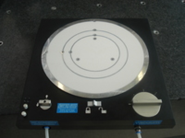
Electronic devices become ever smaller, the functions more extensive. That makes high demands against the finishing techniques of the semiconductor industry, which continues this trend with complex thin techniques. However special operations technologies require extremely thinned out wafer around damages as and/or wafer break to be avoided. Witte Bleckede, manufacturer of different vacuum clamping systems, conceived, designs and manufactures for several years so-called � wafer Chucks � for the semiconductor industry. On the vacuum Chucks those are kept damage-free wafer. The clamping surface consists of a micro-porous material (among other things pure area class 10 suited); under the microstructure very thin materials are fixed absolutely flat and damage-free. Can do evennesses and plan parallelisms of Attack pins, which can be pulled out of the plate, facilitate a placing the wafer within the necessary clamping range. Take off free surfaces, which is absolutely necessary with many evacuated systems, is not necessary here. After treatment those are raised wafer by compressed air-steered Liftings pins with integrated brake mechanics � gently � and can with a Endeffektor taken will picture: Three separated adjustable clamping ranges for wafer of different sizes. Attack pins facilitate the positioning, Lifting pin with brake mechanics lift the wafer ' sanft' on.
This text was translated automatically.

