Purdue University investigates carbon nano-materials with AIXTRON Black liking IC plant
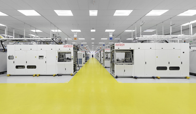
The Birck Nanotechnology center of the Purdue University in west Lafayette, Indiana, the USA ordered a Black liking IC plant in a 2-Zoll-Konfiguration. The incoming orders took place in the fourth quarter 2009, the plant in the second quarter 2010 is delivered. With the new plant carbon nano-materials and High K oxides are separated by means of ALD1) - technology. As professor Peide Ye of the Purdue University confirms, the project is supported in the context of the so-called DURIP program by the US-Verteidungsministerium. The Black Magic CVD/PECVD2) - plant forms thereby the basis for the current research projects of the CMOS3) - characterisation: � this is the first CVD plant, which two different growth modes in an integrated way � with which we thus not only nano-carbon materials and so-called graph, but also High K oxides can separate by means of in-situ-ALD-procedures. " Thus one is able, carbon and oxide-based channel materials for the next element generation to develop further. � the advantage to apply oxides in International Telecommunication Union immediately after channel growth is in the fact that impurities are possibly avoided and we clean channel/oxide boundary surfaces and thus higher performance elements manufacture k�nnen." With the Scifres Nanofabrication Laboratory has in July 2005 opened 58 million US Dollar expensive, 187,000 square meters the large Birck Nanotechnology center a 2500 square meter large pure area for the nano-production of the classes 1-10-100. Beside areas to the nano-structural research, which are shielded against smallest vibrations and are extremely precisely regulated in those temperature and site conditions, there are laboratories for Nanophotonik, crystal growth, molecular electronics, MEMS/NEMS4), surface analysis, SEM/TEM5) - procedures as well as for the following electrical characterisation. With a pronounced cooperative structure the university promotes beyond that the interaction and the technical transfer with the industry in the range of the nanotechnology. Dr. Rainer Beccard, Vice President marketing with AIXTRON: � the use of iii-V connections as channel materials is already a promising beginning, in order to follow moorlands � s Law in the future. Additionally one examines now the possibilities of alternative channel materials on carbon basis. AIXTRONs MOCVD plants for 300 mm wafer� for the production of Iii V Kanalmaterialien worked satisfactorily. With the implementation of the singular CNT /Graphen /ALD plant to the Purdue University also the appropriate research can be operated there now to carbon nano-materials. " 1) ALD, Atomic Layer deposition = Atomlagenabscheidung2) CVD/PECVD, (plasma Enhanced) Chemical vapor deposition = (plasma-supported) gaseous phase separation 3) CMOS, Complementary Metal of oxides Semiconductor = complementary metal oxide semiconductor 4) MEMS, Micro Electro Mechanical of system = micro-electromechanical systems/NEMS, nano- Electro Mechanical of system = nano-electromechanical Systeme5) SEM = secondary electron microscope; TEM = transmission electron microscope�
This text was translated automatically.
