


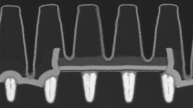
 X-Cut-HAADF-Rasterelektronenmikroskopieaufnahme eines WS2-Bauelements mit einer CPP von 50 nm, einer Kontaktlänge von 19 nm und einer Breite von 256 nm nach dem Ätzen der Gate-Anschlussleitung. Und (B) die entsprechende energiedispersive Röntgenspektroskopie (EDS)-Analyse.")
, die auf demselben 300-mm-Wafer integriert sind, weisen eine gute Anpassung der Schwellenspannung auf.")
-
- Elektronik (Wafer, Halbleiter, Mikrochips,...)
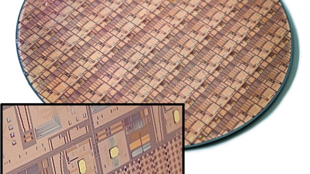
Ein neuartiger 300-mm-Integrationsansatz für Bauelemente auf Basis von 2D-Materialien ermöglicht skalierte n- und p-FETs mit einem contacted poly pitch von 50 nm.
ASML, TSMC und imec machen industrietaugliche Transistoren aus 2D-Materialien durch bahnbrechende 300-mm-Integration greifbarer
– ASML, TSMC und imec stellen einen innovativen 300-mm-Integrationsprozess für Transistoren auf Basis von 2D-Materialien vor, mit dem erstmals skalierte n- und p-FETs mit einem Kontaktabstand (CPP) von 50 nm realisiert werden, die mittels EUV-Lithografie strukturiert wurden.
– Bei den skalierten nFET…


 und Barriere- (B) Gates von knapp 6 Nanometern, ermöglicht durch High-NA-EUV-Lithografie. Das Bild zeigt außerdem die Akkumulations- (A) und Einschluss- (C) Gates.")


 Schematische Darstellung der auf drei Wortleitungen basierenden 3D-CCD-Struktur: unteres Gate (BG), mittleres Gate (CG) und oberes Gate (TG), wobei sich das Source (S) unten und das Drain (D) oben befinden; (b) TEM-Querschnittsbild, das drei Gate-Schichten mit einem Wortleitungsabstand von 80 nm zeigt.")
 Darstellung des Ansteuerungsschemas über drei Gates für den seriellen Ladungstransfer in einem 3D-CCD-Speicher mit drei Wortleitungen; (b) Schematische Darstellung des 3D-CCD-Betriebs, die den Elektronentransfer durch die Bildung und Verschiebung von Potentialmulden unter den Gates veranschaulicht.")
 I-f-Kennlinien von 7 Bauelementen mit unterschiedlichen Durchmessern des Memory Holes (MH), gemessen bis zu 4 MHz; (b) die Anzahl der pro Zyklus übertragenen Elektronen, ermittelt aus der Steigung der entsprechenden I-f-Kurven.")

")
")


, Thomas Skordas (European Commissioner), Luc Van den hove (CEO imec), Henna Virkkunen (European Commissioner), Matthias Diependaele (MP Flanders), Jari Kinaret (Executive Director Chips JU), Christophe Fouquet (CEO ASML).")


 auf der oberen/unteren Ebene befinden und über die entsprechenden Verbindungen verfügen. / A 4x4 IGZO 2T0C cell array where read/write transistors (RTX/WTX) are on top/bottom levels with the corresponding connections.")


