

- Electronics (wafers, semiconductors, microchips,...)
- Translated with AI
Imec demonstrates the extension of chemically amplified resists for High NA EUV lithography
Imec and its material suppliers optimize their chemically amplified resist (CAR)-based platforms toward High NA EUV single patterning of 22nm pitch line structures supporting A14/A10 logic designs
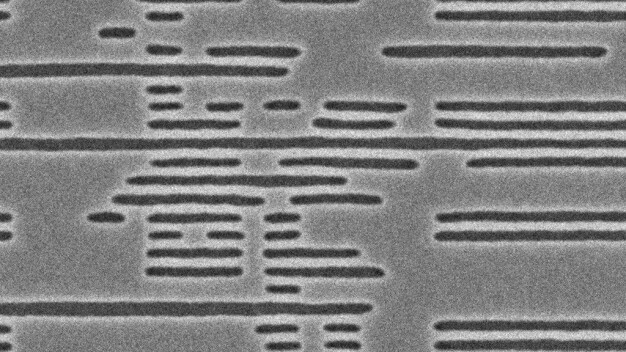
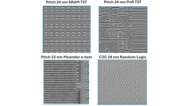
Figure 1. Representative 0.55NA EUV wafer SEM images showing CAR patterning on tight-pitch logic metal and via structures, including SRAM (AEI), PnR (AEI), meander e-test (ADI), and 28nm C2C random logic vias (ADI) (AEI = after etch inspection; ADI = after development inspection).
– Imec optimizes CAR-based technology for the High NA EUV single patterning of several layers of the A14/A10 logic technology nodes.
– A variety of tight-pitch logic metal line and via structures have been demonstrated, including meander and forked e-test structures down to 22nm pitch, 24nm SRAM layouts at 26nm tip-to-tip (T2T), 24nm place-and-route structures with 28nm T2T, as well as random logic via features at 28nm center-to-center distance.
– “CAR is a well-established resist platform with proven stability and manufacturability. We have shown for the first time that we can extend CAR-based technology into the High NA EUV single patterning regime.” – Geert Vandenberghe, imec.
– These breakthrough results, achieved in tight collaboration with ASML, imec’s material suppliers and its broader patterning ecosystem, reinforce imec’s position as the industry’s launchpad into the ångström era.
At 2026 SPIE Photomask Technology + EUV Lithography Conference, imec, a world-leading research and innovation hub in advanced semiconductor technologies, demonstrated the feasibility of patterning tight-pitch random logic structures after a CAR-based single-print High NA EUV lithography step. Logic structures include lines/spaces down to 22nm pitch, and vias at 28nm center-to-center distance. These breakthrough achievements show that the well-established CAR resist technology can be used for the High NA EUV single patterning of several layers of the A14/A10 logic technology nodes. The results, achieved in tight collaboration with ASML, imec’s material suppliers and its broader patterning ecosystem, underscore imec’s position as the industry’s gateway to the ångström era.
High NA EUV lithography is a key technology for continuing the dimensional scaling path and leading industry into the ångström era – a need arising from the high demands imposed on compute density in future AI and HPC systems. According to imec’s latest logic technology roadmap, High NA EUV lithography insertion is anticipated for the A14/A10 logic node, where achieving reliable patterning at aggressive pitches is critical. It is therefore also a key enabling technology for the imec-hosted European NanoIC pilot line, which is targeting beyond 2nm systems-on-chip. Imec, ASML and its partners in patterning are accelerating High NA EUV’s industrial adoption by taking a holistic approach, i.e., by co-optimizing the entire patterning ecosystem. This includes, among others, validating novel resist materials and processes, etch techniques etc, while simultaneously pushing the performance of the existing chemically amplified resist (CAR)-based technology.
With initial e-test results shown at the 2026 IEEE International Interconnect Technology Conference (IITC), imec and its material suppliers validated the feasibility of CAR-based High NA EUV single-patterning on 28nm pitch line structures – exceeding the limit of what was believed possible with CAR-based approaches. Showing promising combo yields on 1.8m long metallized e-test structures, this work has laid the foundation for further optimization of CAR resist and etch chemistries.
At the 2026 SPIE Photomask Technology + EUV Lithography, imec now shows for the first time the extended use of CAR resists towards patterning 22nm line/spaces after a single High NA EUV exposure step. Good pattern fidelity was achieved on meander and forked e-test structures down to 22nm pitch. In addition, a variety of tight-pitch logic metal and via structures could be demonstrated, relevant for advanced node random logic designs: 24nm SRAM layouts at 26nm tip-to-tip (T2T), 24nm place-and-route structures with 28nm T2T, as well as random logic via features at 28nm center-to-center distance. These results pave the way for industry to continue using CAR in combination with High NA EUV lithography for the single patterning of some of the critical layers of the A14/A10 logic nodes, including the metal-2 layer, via layer, and metal-to-diffusion (MD) layer (the layer that connects source/drain diffusion layers up to the first metal layer).
Geert Vandenberghe, VP R&D for Patterning Technology Programs at imec: “We have shown that we can extend CAR-based technology, achieving pitches that were not accessible with CAR-based single-print 0.33NA EUV lithography. CAR-based patterning is a well-established technology that has served the semiconductor industry for several decades, with proven stability and manufacturability. Our data proves that it remains highly valuable for the High NA EUV lithography era, giving our strong ecosystem of partners a decisive advantage when entering the ångström era. This breakthrough achievement was made possible through tight collaboration with our ecosystem partners, primarily involving the co-optimization of CAR materials and litho-etch techniques together with our material suppliers. It has laid the groundwork for further optimizations, driving yield improvement and pushing CAR performance towards even more aggressive pitches.”
The results will be presented at the 2026 SPIE Photomask Technology + EUV Lithography Conference in paper 14272-8 – Why chemically amplified resists extension is critical for early High-NA EUV insertion into HVM?, B. Baskaran et al.
IMEC Belgium
3001 Leuven
Belgium