

- Electronics (wafers, semiconductors, microchips,...)
- Translated with AI
Fraunhofer IPMS presents new technologies for the semiconductor industry of tomorrow
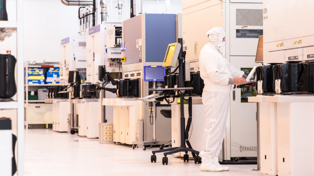
300 mm cleanroom at Fraunhofer IPMS. © Fraunhofer IPMS
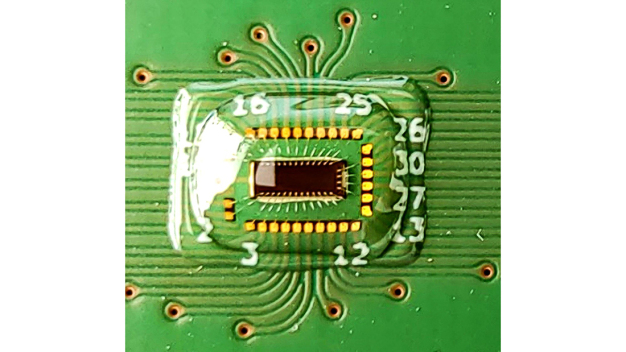
8 kbit FeMFET demonstrator developed by Fraunhofer IPMS as a chip-on-board solution. © Fraunhofer IPMS
At SEMICON Europa 2026, the Fraunhofer Institute for Photonic Microsystems IPMS presented current research findings and technological developments for the semiconductor industry. The focus was on solutions that open up new avenues for integrating diverse technologies, reduce the energy consumption of electronic systems and increase the performance of future applications. The spectrum ranges from new manufacturing and integration approaches to innovative components and system technologies.
How can different chip technologies be efficiently connected? How can memory become more energy-efficient? And what opportunities do photonic technologies offer for data processing and sensing? Fraunhofer IPMS presented answers to these questions at SEMICON Europa 2026 in Munich.
The trade fair presentation brought together current work from the European pilot lines APECS and FAMES. “Future semiconductor systems will increasingly be defined by the interaction of specialized components. The key is to integrate chiplets, for example with memory or photonic functions, efficiently and to test the processes required for this under conditions close to industrial production. Back-end process technologies are also making their way into the front-end manufacturing of highly complex chips. Together, these approaches can give rise to powerful and energy-efficient systems,” said Prof. Wenke Weinreich, Director of the Fraunhofer IPMS.
APECS pilot line: Heterogeneous integration for future semiconductor systems
APECS stands for “Advanced Packaging and Heterogeneous Integration for Electronic Components and Systems.” The European pilot line is part of the “Chips for Europe” initiative under the EU Chips Act. It is being established under the leadership of the Research Fab Microelectronics Germany, or FMD for short, with the participation of additional European partners.
The goal of APECS is to provide companies with access to technologies for advanced packaging and heterogeneous integration under conditions close to industrial production. The aim is to combine different semiconductor components, such as chiplets, memories, sensors or photonic components, into high-performance overall systems. As a member of the FMD consortium, Fraunhofer IPMS contributes its expertise in wafer processing, integration technology and system development to the pilot line.
Interposers and 2.5D integration
One approach to heterogeneous integration is 2.5D integration. In this process, several chiplets are arranged next to one another on what is known as an interposer, which is positioned on a substrate like a conventional chip. The interposer serves as a high-density connection layer between the individual components and enables short, high-density electrical connection paths. Different functions that require a high level of data exchange, such as sensors and memories, can therefore be manufactured as separate chiplets using different technologies. Connecting them via an interposer enables data exchange comparable to integration on a single chip. In this way, computing logic, memory and specialized functions can, for example, be combined modularly in a compact system. Unlike 3D integration, the components are not stacked vertically, but arranged next to one another on the interposer.
Fraunhofer IPMS is developing process and integration technologies for this purpose on 200 mm and 300 mm wafers. This work provides a foundation for scalable chiplet systems and complex heterogeneous system architectures.
Quasi-monolithic integration of chiplets at wafer level
With quasi-monolithic integration, or QMI for short, Fraunhofer IPMS is pursuing another approach to high-density chiplet integration. In this process, chiplets are embedded in specially structured recesses in a silicon wafer, known as pockets. The surface is then planarized and prepared for subsequent wafer-level wiring.
As part of the APECS pilot line, Fraunhofer IPMS has demonstrated for the first time that chiplets can be integrated into a silicon wafer in this way. This marked the achievement of the first critical milestone on the QMI roadmap.
The approach combines the modularity of chiplet systems with the high integration density of wafer-based manufacturing. This allows different chip components to be brought together in a common manufacturing process.
Integrated platform for the photonic systems of the future
Whether for sensing, data processing or quantum technologies: integrated photonics provides the basis for compact and high-performance systems. Fraunhofer IPMS develops electro-optical components and associated CMOS-compatible manufacturing technologies on 200 mm and 300 mm wafers. A central technology platform is the silicon nitride waveguide platform (SiN), which is available for both wafer sizes. It is characterized by very low optical losses across a broad wavelength spectrum ranging from the visible to the mid-infrared and thus enables the realization of complex photonic circuits. This platform forms the basis for highly sensitive photonic biosensors as well as applications in photonic computing, quantum technologies and the hybrid integration of active components. Electronic and optical functionalities are integrated at wafer level, allowing the resulting components to be manufactured cost-effectively in large quantities.
Ferroelectric memories for fast and energy-efficient electronics
Building on many years of research programs, Fraunhofer IPMS provides ferroelectric memory technologies based on hafnium oxide for energy-efficient microelectronic systems as part of its pilot line offering. The technology portfolio includes non-volatile FRAM and FeFET technologies, including reference designs for embedded data memories and AI accelerator circuits. The focus is on the further development of components and process modules, as well as their integration into established semiconductor manufacturing processes.
The memory technologies operate at supply voltages below one volt and enable switching times in the nanosecond range. They combine the non-volatile storage of information with high endurance and reliability. Specially developed ferroelectric layer stacks from Fraunhofer IPMS help ensure the performance and stability of the components even under demanding operating conditions, such as elevated temperatures.
This makes the technologies particularly suitable for embedded applications, intelligent sensor systems and energy-efficient edge computing solutions where fast data processing, low energy consumption and permanent data storage are required in the smallest possible space.
External partners and interested parties gain access to the technology platforms, including design access. They can place their own circuit designs and test structures, have them manufactured and evaluate them for application-specific solutions or demonstrators. Fraunhofer IPMS provides support ranging from design adaptation and manufacturing to the electrical characterization of the components.
Fraunhofer IPMS at SEMICON Europa 2026
The work demonstrates the breadth of the technology and manufacturing expertise available at Fraunhofer IPMS: from the development of new materials and components and manufacturing processes on 200 mm and 300 mm wafers to the integration of complex heterogeneous systems. “For microelectronics in Europe to remain competitive, new technologies must make the transition from research to application. Reliable process chains and opportunities for testing under conditions close to industrial production are crucial for this,” Prof. Weinreich concludes.
Fraunhofer-Institut für Photonische Mikrosysteme IPMS
01109 Dresden
Germany