



New year, new job? View the vacancies! More ...
Vaisala ClearClean Piepenbrock Hydroflex


All publications from IMEC Belgium

  • Electronics (wafers, semiconductors, microchips,...)

A major milestone in propelling industry into the ångström era

Imec receives the world’s most advanced High NA EUV system

– Imec announces the arrival of the ASML EXE:5200, the world’s most advanced High NA EUV lithography system, in its 300mm cleanroom in Leuven. 
– Operating the High NA EUV system in direct connection with state-of-the-art metrology and patterning equipment/materials accelerates learning cycles to unlo…

  • Electronics (wafers, semiconductors, microchips,...)

New advanced interconnect PDKs pave the way for high‑density, energy‑efficient chip‑to‑chip integration.

NanoIC opens access to first-ever fine-pitch RDL and D2W hybrid bonding interconnect PDKs

On 2nd March 2026 the NanoIC pilot line, a European initiative coordinated by imec and dedicated to accelerating innovation in chip technologies beyond 2nm, released two first-of-a-kind advanced interconnect process design kits (PDKs): a fine-pitch redistribution layer (RDL) and die-to-wafer (D2W) h…

Left to Right: Patrick Vandenameele (CEO-elect imec), Thomas Skordas (European Commissioner), Luc Van den hove (CEO imec), Henna Virkkunen (European Commissioner), Matthias Diependaele (MP Flanders), Jari Kinaret (Executive Director Chips JU), Christophe Fouquet (CEO ASML).
  • New building

Imec celebrates Europe's NanoIC pilot line with the official opening of a 2,000 m² large cleanroom extension on its campus in Leuven.

Imec inaugurates NanoIC pilot line, accelerating innovation in sub-2nm systems-on-chip

– Imec inaugurates Europe’s NanoIC pilot line with the official opening of a 2,000m² cleanroom expansion at its Leuven campus.
– Equipped with cutting-edge tools, including ASML’s High NA EUV tool, imec’s cleanroom is a cornerstone of the NanoIC initiative – pursuing sub-2nm chip technology.
– Exactly four…

3D representation of the A14 device structure showing the 4 stacked nanosheets with its local routing and back side metal contact. A 4x4 IGZO 2T0C cell array where the read/write transistors (RTX/WTX) are located on the top/bottom levels with the corresponding connections.
  • Electronics (wafers, semiconductors, microchips,...)

Launch of new A14 and embedded DRAM process design kits (PDKs) accelerates research and innovation in logic and memory scaling

NanoIC extends its PDK portfolio with first A14 logic and eDRAM memory PDK

On 2nd February, 2026, the NanoIC pilot line, a European initiative coordinated by imec and dedicated to accelerating innovation in chip technologies beyond 2nm, announced the release of two new process design kits (PDKs): an A14 pathfinding PDK for advanced logic scaling and an eDRAM system explora…

Photos of the Veeco 300-mm oxide system for hybrid-MBE BTO on Silicon epitaxy. Cross-sectional Transmission Electron Microscopy image of the BaTiO₃/SrTiO₃/Si(001) heterostructure with high-resolution micrograph and atomic force microscopy images in inset.
  • Electronics (wafers, semiconductors, microchips,...)

First-Of-Its-Kind Solution For Barium Titanate Epitaxy on Silicon to Accelerate Datacom and Quantum Computing Applications.

Veeco and imec develop 300mm compatible process to enable integration of barium titanate on silicon photonics

Veeco Instruments Inc. (Nasdaq: VECO) and imec announced today that they have collaboratively developed a 300mm high volume manufacturing compatible process that enables the integration of barium titanate (BaTiO3 or BTO) on a silicon photonics platform. BTO is a promising material with unique electr…

The cleanroom at Imec forms the basis for NanoIC's PDKs, which are based on 2-nm process flows. (Image: Imec) / Imec's cleanroom provides the foundation for NanoIC's PDKs, based on 2 nm process flows. (Photo: Imec)
  • Workshop / Course

Major update of NanoIC’s Pathfinding N2 P-PDK empowers researchers and designers to learn and innovate on full SoC architectures

NanoIC adds advanced SRAM memory macros to its N2 pathfinding PDK

NanoIC pilot line, a European initiative coordinated by imec and dedicated to accelerating innovation in chip technologies beyond 2nm, announces the release of the N2 P-PDK v1.0, an important update of its N2 Pathfinding Process Design Kit (P-PDK). This new version introduces several new features, i…

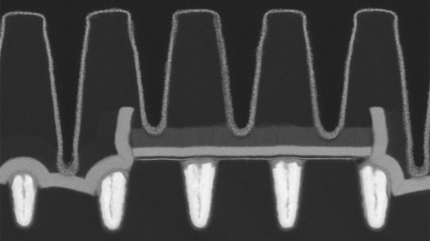
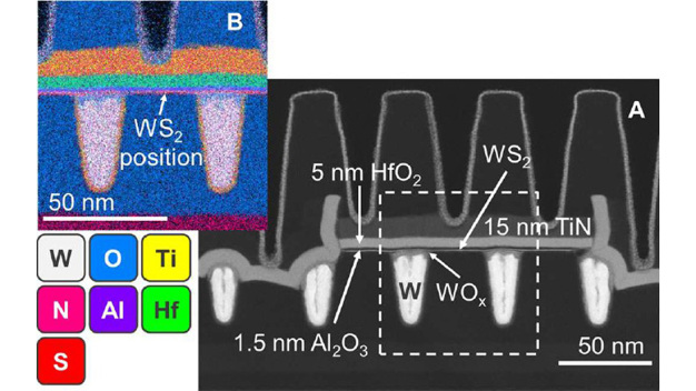
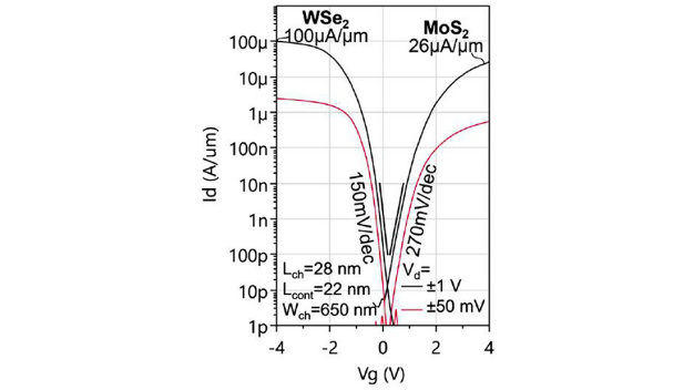
Figure 1 – (Left) Transfer curves of 2D-pFET devices using defect-passivated synthetically-created bi-layer WSe2 films, with the best device showing Imax = 690µA/µm; (Right) TEM cross-section of the finalized dual-gated 2D pFET (Lch=channel length; TG=Top Gate; BG=Back Gate; S=Source; D=Drain; IL=Interlayer), in collaboration with TSMC. Figure 2 – (a) Dry etching into SiO₂; (b) Dry and wet etching, which stops selectively on the WS₂ monolayer channel, also removing the AlOx interlayer laterally along the entire channel length (in collaboration with Intel).
  • Electronics (wafers, semiconductors, microchips,...)

Collaboration with leading semiconductor manufacturers pivotal in optimizing the key modules for 2D-material device integration

Imec advances 2D-material based device technology beyond state of the art in support of the future logic technology roadmap

– Imec, in collaboration with leading semiconductor manufacturers, addressed key challenges in advancing 2D-material device technology, which is considered a long-term option for extending the logic technology roadmap.
– Collaboration with TSMC resulted in record performing WSe2 -based pFETs (with I…

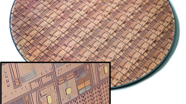
Imec pioneers full wafer-scale (300mm) production of solid-state nanopores with EUV lithography, as shown in the photo. © imec Cross-sectional and top-view TEM of the fabricated solid-state nanopore. Cross-sectional and top-view TEM of the fabricated solid-state nanopore.
  • Electronics (wafers, semiconductors, microchips,...)

Breakthrough enables scalable, high-precision biosensing applications in life sciences and healthcare

Imec demonstrates first wafer-scale fabrication of solid-state nanopores using EUV lithography

1. Imec has achieved the first successful wafer-scale fabrication of solid-state nanopores using EUV lithography on 300mm wafers. This innovation transforms nanopore technology from a lab-scale concept into a scalable platform for biosensing, genomics and proteomics.
2. Nanopores are hailed as gamech…

The cleanroom at Imec forms the basis for NanoIC's PDKs, which are based on 2-nm process flows.
  • Workshop / Course

Major update of NanoIC’s Pathfinding N2 P-PDK empowers researchers and designers to learn and innovate on full SoC architectures.

NanoIC adds advanced SRAM memory macros to its N2 pathfinding PDK

This week, at SEMICON Europe, the NanoIC pilot line, a European initiative coordinated by imec and dedicated to accelerating innovation in chip technologies beyond 2nm, announces the release of the N2 P-PDK v1.0, an important update of its N2 Pathfinding Process Design Kit (P-PDK). This new version…

Better informed: With YEARBOOK, NEWSLETTER, NEWSFLASH, NEWSEXTRA and EXPERT DIRECTORY

Stay up to date and subscribe to our monthly eMail-NEWSLETTER and our NEWSFLASH and NEWSEXTRA. Get additional information about what is happening in the world of cleanrooms with our printed YEARBOOK. And find out who the cleanroom EXPERTS are with our directory.

Buchta Pfennig Reinigungstechnik GmbH Becker HJM