

New year, new job? View the vacancies! More ...
PMS Piepenbrock Buchta Pfennig Reinigungstechnik GmbH


All publications from Fraunhofer-Institut für Photonische Mikrosysteme IPMS

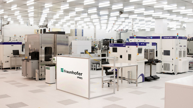
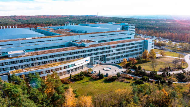
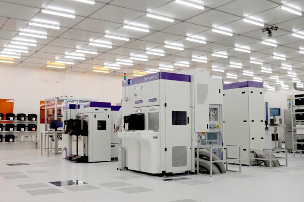
300 mm cleanroom at the Fraunhofer IPMS. © Fraunhofer IPMS Aerial view of Infineon Dresden. © Infineon Technologies AG / Aerial view of Infineon Dresden. © Infineon Technologies AG
  • mobility of the future

Intelligent energy management for the future

Fraunhofer IPMS supports the 300 mm process development of smart power technologies for the semiconductor manufacturer Infineon at the Dresden site

In a joint development project spanning around one year, important progress was made in the production of “Smart power technologies”. Fraunhofer IPMS provided significant support to the semiconductor manufacturer Infineon by supplying selected process modules within the entire CMOS process value cha…

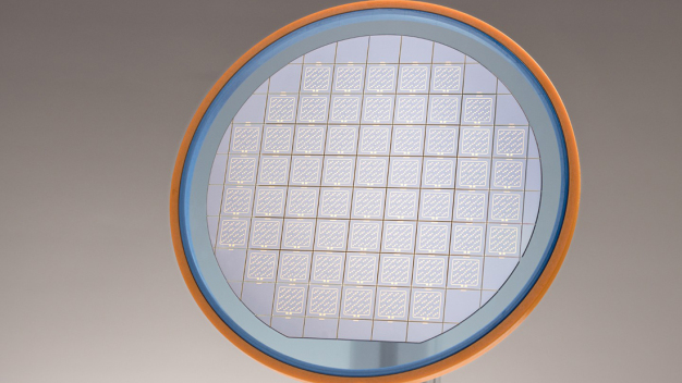
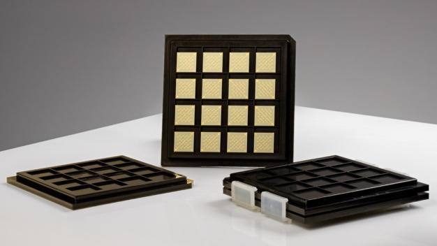
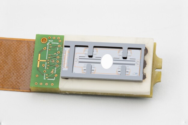
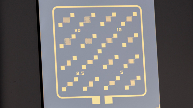
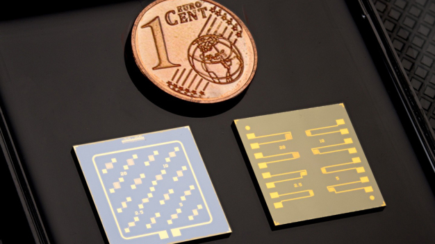
Individual OFET substrates from Fraunhofer IPMS. © Fraunhofer IPMS / Diced OFET substrates from Fraunhofer IPMS. © Fraunhofer IPMS OFET substrate from Fraunhofer IPMS as wafer. © Fraunhofer IPMS / OFET substrates from Fraunhofer IPMS as wafer. © Fraunhofer IPMS OFET substrate from Fraunhofer IPMS in a waffle pack. © Fraunhofer IPMS / OFET substrates from Fraunhofer IPMS in a waffle pack. © Fraunhofer IPMS
  • Electronics (wafers, semiconductors, microchips,...)

Substrates for organic field-effect transistors (OFET) for the development of high-tech materials

Customized silicon chips from Saxony for material characterization of printed electronics

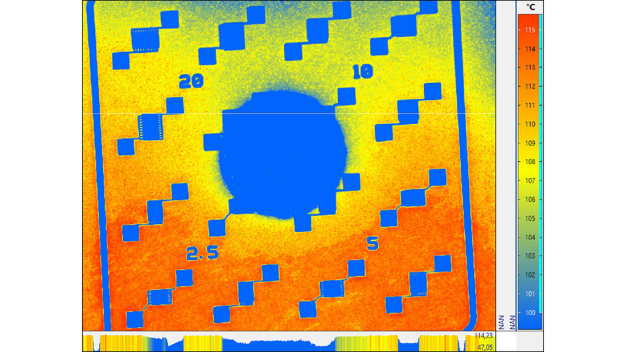
How efficient are new materials? Does changing the properties lead to better conductivity? The Fraunhofer Institute for Photonic Microsystems IPMS develops and manufactures silicon substrates for this purpose. This enables the fundamental electrical characterization of materials such as a novel grap…

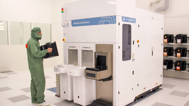
eBeam metrology equipment from Applied Materials in the cleanroom of Fraunhofer IPMS. © Fraunhofer IPMS / Applied Materials' eBeam metrology equipment at cleanroom of Fraunhofer IPMS. © Fraunhofer IPMS
  • Electronics (wafers, semiconductors, microchips,...)

Launch of European Semiconductor- Metrology Technology Hub

Applied Materials and Fraunhofer IPMS launch European Semiconductor- Metrology Technology Hub

– New hub will provide state-of-the-art metrology systems to accelerate semiconductor research and enhance development projects with chipmakers and ecosystem partners across Europe, particularly in ICAPS* market segments
– Collaboration to accelerate learning, develop novel methods and prove new met…

Better informed: With YEARBOOK, NEWSLETTER, NEWSFLASH, NEWSEXTRA and EXPERT DIRECTORY

Stay up to date and subscribe to our monthly eMail-NEWSLETTER and our NEWSFLASH and NEWSEXTRA. Get additional information about what is happening in the world of cleanrooms with our printed YEARBOOK. And find out who the cleanroom EXPERTS are with our directory.

C-Tec Becker ClearClean MT-Messtechnik