


- Company
Jenoptik will more than double on-site production capacity for its micro-optics business in Dresden
The Group plans to invest around 70 million euros in a highly functional cleanroom facility. Construction will begin in 2022 – production to start in early 2025.
The Jenoptik Group intends to build a state-of-the-art production building with office complex in Dresden. In total, the photonics group is planning to invest around 70 million euros in a cleanroom facility for micro-optics and sensors for semiconductor equipment. Jenoptik acquired a 24,000-square-meter plot of land in the Airportpark Dresden in May 2021, and since then has planned and designed further details of the buildings. In addition to the highest cleanliness and vibration requirements for cleanroom production, the project also focuses on ecological and social aspects – in parallel, Jenoptik seeks sustainability certification for the project.
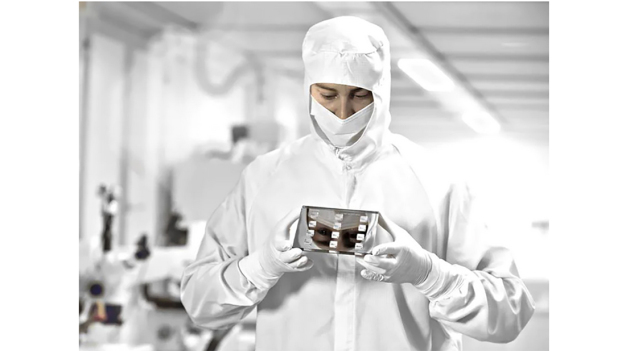
“We consciously intend to make the investment for our micro-optics business in Germany, and specifically Dresden, the country’s Silicon Valley, an outstanding location for the semiconductor industry,” says Jenoptik President & CEO Stefan Traeger. Dresden is Europe’s key location for the semiconductor industry, home to a large number of global companies and research institutes operating in this industry. Jenoptik has been operating here since 2007, manufacturing micro-optics and sensors for use in semiconductor lithography systems. Unlike traditional optics, these high-precision components are also manufactured in a process similar to semiconductor production.
“The new fab will allow us to pool and more than double our on-site production capacity,” says Stefan Traeger. Construction is due to begin in 2022, with production starting in early 2025. A further 60 high-tech jobs at the Dresden site will then be added to the present 50.
The micro-optics and sensors manufactured here are core components for current and future lithography technologies (DUV and EUV), enabling more compact chip structures and thus greater computing power with an even smaller design. Semiconductor growth is particularly being driven by the expansion in data communications and IT, but also by automotive and other industrial applications such as the Internet of Things, artificial intelligence, etc.
“The construction of the state-of-the-art facility in Dresden is to further boost Dresden’s appeal in the heart of Silicon Saxony. I would like to take this opportunity to assure you of the express commitment of Dresden, the state capital, to support the planned completion of this ambitious project,” says Dirk Hilbert, the mayor of Dresden, on Jenoptik’s investment.
JENOPTIK AG
07743 Jena
Germany


